Intel 960 con-badge
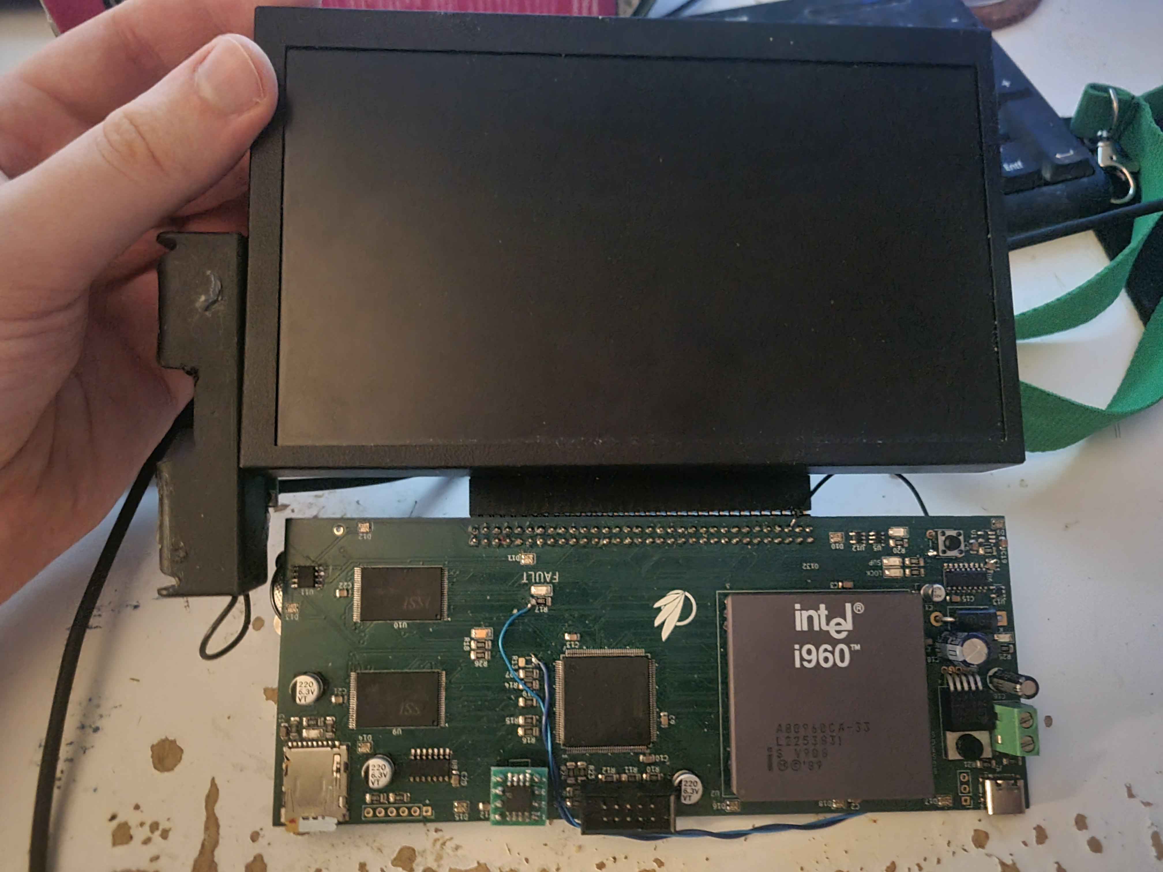
Yep, that’s the proper orientation for it: PCB below the screen.
Just like every year, EF30 meant another year, another badge. This time, I had a lot of (perhaps lofty goals), mostly to do with fixing a lot of the flaws previous badges had. If you’re wondering why you haven’t heard about the badge I built in-between the i386 badge and this one, its because it was an absolute mess that required 3 revisions and hundreds of euros of wasted components to get to work at all. Its not my proudest work. On top of that, programming everything in assembly was taking its toll on me, so the primary goal this year was this: switch to using C. Technically, the i386 badge could already do this, but it had a lot of issues with its electronics, another point worth addressing. It was also what made me decide to never touch x86 ever again, but that doesn’t mean I have to say goodbye to Intel just yet.
Intel actually used to be quite good at hating their own architecture, releasing a number of competing ones. The laughable iAPX and headspinning Itanium are the most well known, but they also released two more obscure architectures: the i960 and the i860 (which actually released after the former, despite the lower number). And, of course, I would never pass up the opportunity to work with an obscure architecture. On top of that, the i960 is even RISC! Or, well, what Intel considers to be "RISC". Looking at the mess that is x86, that bar is pretty low.
Hardware selection
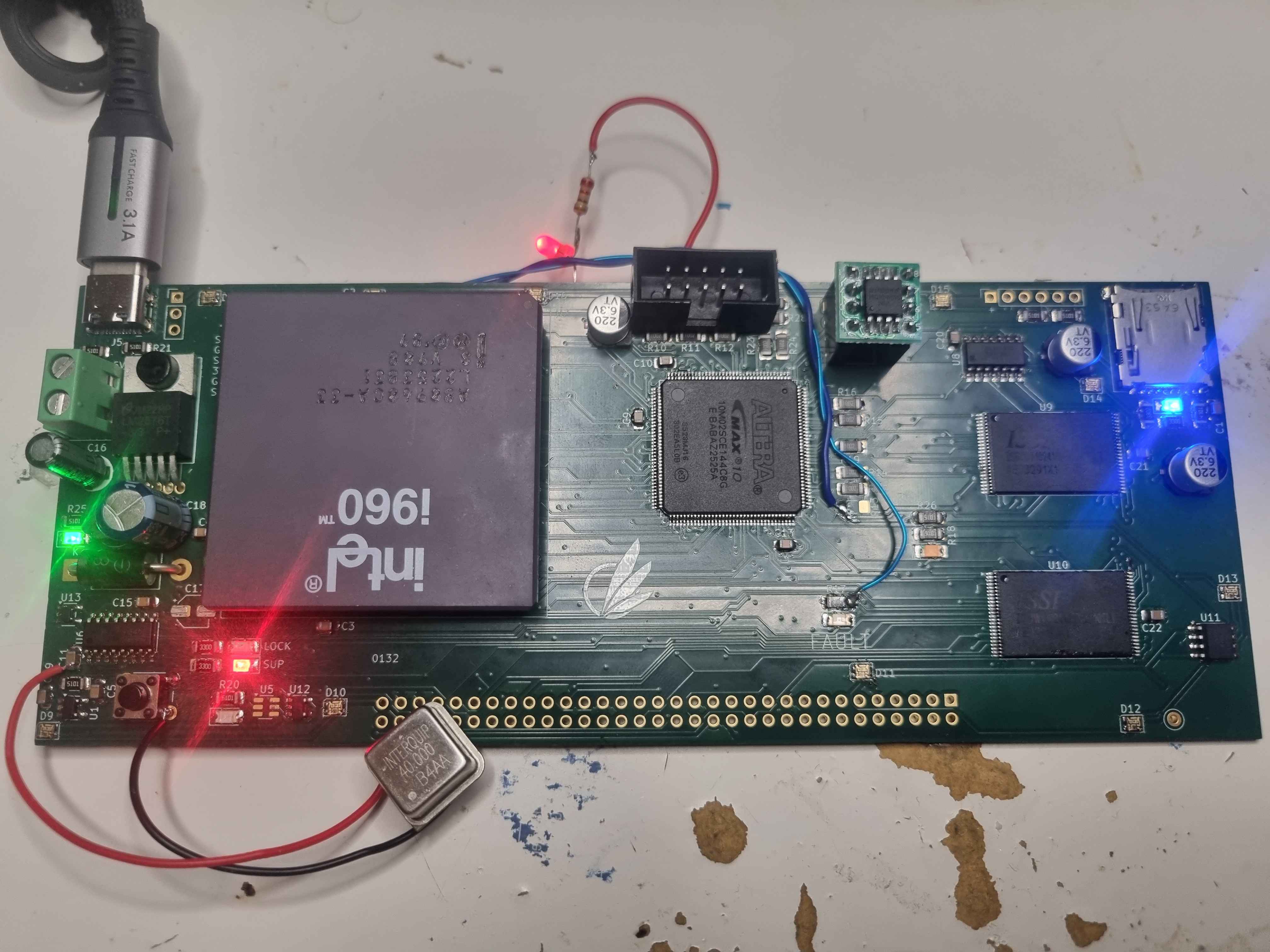
The past badges I’ve built all had the problem of bloated part counts making layout difficult. One thing that came out of my failed last year’s badge is that it allowed me to experiment with concentrating more functionality into a cheap FPGA. A MAX 10 series, which I used again here, this time for everything except video. Compare this to the i386 badge, which had two programmable logic devices and a bunch of discrete logic glue.
The FPGA on this board contains a UART, SPI port, GPIO and timers, as well as handling the addressable LEDs, micro SD card for storage, SPIFLASH for boot code, and bus glue logic (which actually needs to be a state machine for the i960 bus).
Most interestingly, the bus signaling of the i960 is so similar to the i486, I actually dare to make the claim that its the exact same circuitry inside the chip. This would actually track, as the versions of the i960 with an IMU do memory mapping the exact same as x86 processors of the time, down to the exact terminology and register definitions, indicating it is the same IP.
Storage may appear to have downgraded in bandwidth, going from CompactFlash to a SD card in SPI mode, but I found the bandwidth sufficient in my testing. However, RAM will be upgraded to 4MiB, the most of any badge so far. This will hopefully allow me to do a more advanced 3D rendering demo as well as utilize complete framebuffers in my image decode algorithms. I’ve also added a I²C RTC chip on a software bit-banged I²C port with backup battery to show the current time in the corner of the display. And finally, the star of the show: a ceramic Intel i960 CPU. Upside down, because the datasheet lied to me about the location of the Pin 1 marker!
Originally, a more complex power supply solution was planned, but it slowly devolved back into two 18650s, one for the display, one for the CPU. Good thing this time is that this is a RISC CPU, and despite the more complex pipelined architecture, it consumes way less power than the i386. I was able to keep the 18650s topped off faster than the badge discharged them, even with the high power draw of the display.
Video Interface
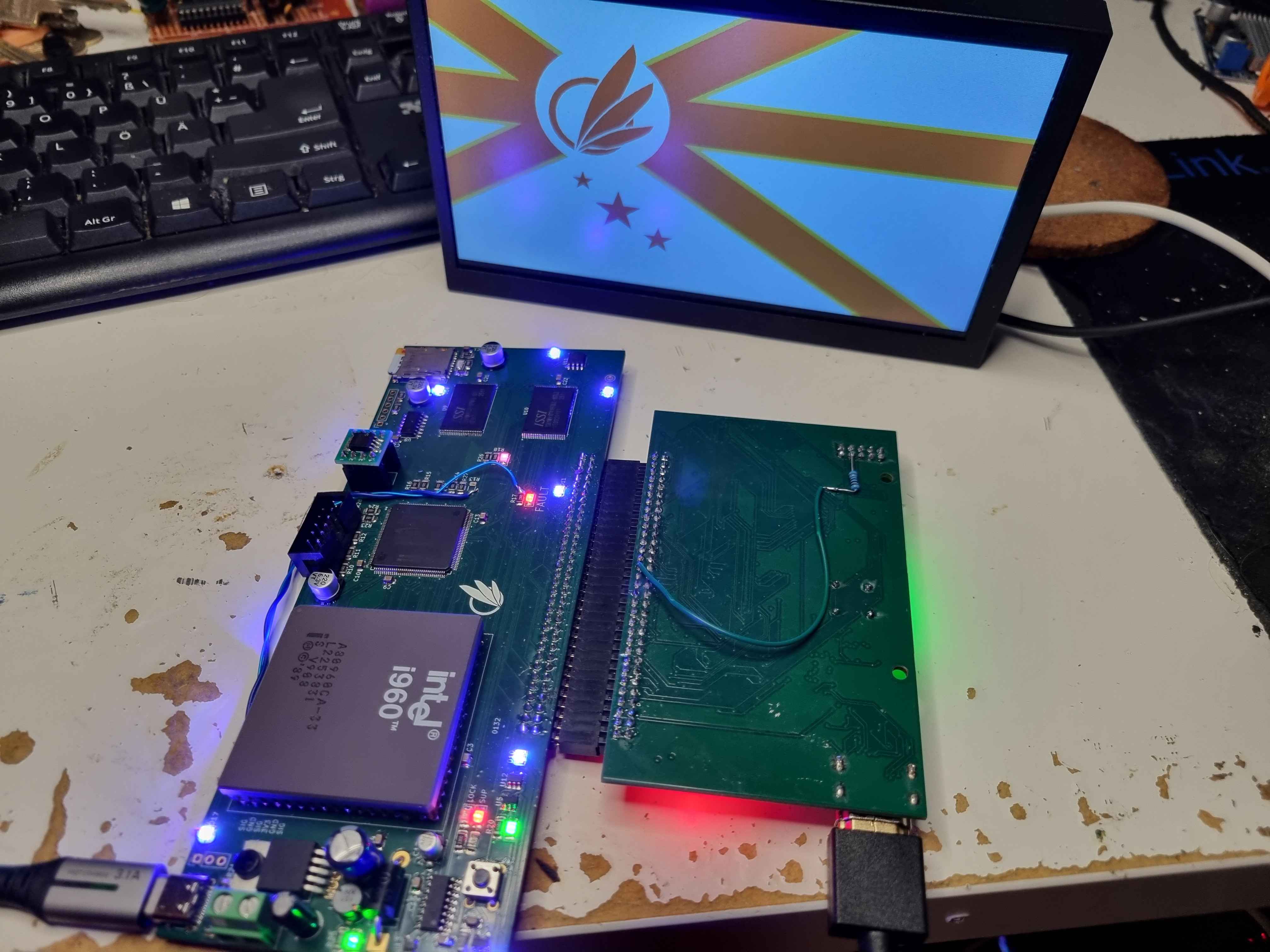
I’ve neglected to mention video so far and there doesn’t even appear to be any circuitry for it on the picture above, but this is because its received a massive upgrade. Instead of an embedded TFT display, I’ve acquired a straight-up monitor. A physically small one, but with a 1024 by 600 resolution and VGA, HDMI and Composite inputs. It increases the total weight of the badge to over 1.1 kilogramms, but a standard lanyard and my neck can handle it, I’m sure. Now, I could’ve easily just used the VGA port. VGA signaling is easy to generate, though I wanted to continue to use full 24-bit color and implementing the DACs for that seemed difficult. So, I instead settled on trying to use HDMI for the first time, using the ADV7513. This chip accepts VGA-like sync signals, but with dedicated pixel clock and blanking inputs, and a 24-bit color data input, and throws out a HDMI signal.
Expecting this to be the most difficult part of the project, I rolled a test PCB with just the ADV7513 and hooked it up to a FPGA board to try it, only for it to work quite easily. For the full board, however, which would require two memory chips, I decided to design a dedicated PCB that would plug in to and below the CPU motherboard, becoming hidden behind the display. This does mean half of the electronics won’t get shown off, but also meant not having to re-built this circuitry if a new revision of the CPU board was needed, as well as making the CPU board slimer, thus resulting in a more aesthetic PCB-to-screen-ratio (also something I’d been struggling with). This time, the mentioned video memory will actually be directly exposed to the CPU bus, with a number of bus buffers and latches present to make it happen. The CPLD that I put on the video board to generate the memory addresses and video timings links up to the FPGA on the CPU board, holding bus accesses during active display periods (the FPGA just pauses the CPU clock during access latencies instead of using the READY input, as I found this easier to implement).
The one annoying thing was that the ADV7513 requires its internal registers to be set up over I²C before it does anything. I could have programmed the i960 to take care of this, but that’d mean additional boot time and several seconds before the display actually detected the valid signal and turned on, so I decided this would finally allow me to use one of those 3-cent microcontrollers, the PMS150C, to bit-bang out the initial configuration to the ADV7513 over I²C in parallel to the i960 resetting and going through its initial bootloader steps.
In my infinite wisdom, however, I did not put enough memory onto the video board to double-buffer. On top of that, it turns out that all the horizontal and vertical display blanking periods added together for one frame are not enough time to fully update all frame buffer contents. If the i960 just fills the whole buffer with one color, it still takes over a second to complete. Worse if it copies from a framebuffer in main memory, which was the intended solution here. For a slideshow, this is okay, but I was certainly not going to produce any demos or games on this system. This makes this the third badge where the NES Controller input goes unused. Go figure.
Software architecture
Bootloader
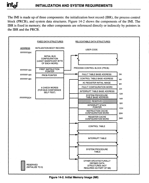
Intel i960: reseting has never been this hard!
Just like other Intel CPUs, the i960 just has to be a bit special when it comes to booting. It expects a whole datastructure with configuration data and pointers to other data structures to be present at the end of memory. Most important is the PRCB. You see, the i960 segments memory, but the segments are fixed. The address space is split into 256MiB segments and each has its own bus configuration. At least the bus is configurable, allowing me to adjust all kinds of wait states to make my system work. A few of them are unnecesary. The SRAM is technically fast enough to respond to the CPU in one clock cycle, but a single wait state is required to generate the correct signaling to make writes work reliably. Oh well.
The bootloader is actually written in C after just a short snippet of assembly, and stored in the SPIFLASH. But getting the CPU to be okay with the slow SPIFLASH accesses seemed difficult. Or maybe it was a problem with my SPIFLASH interface on the FPGA. In either case, the easier solution than debugging all that was to have the FPGA copy the first 8KiB from the SPIFLASH into its BRAMs and then expose that to the CPU.
The bootloader barely fits into 8KiB! The rest of the flash is taken up by the boot logo. The code just initializes the SD Card, then copies a bunch of blocks from it into SRAM to jump to. This time, I actually included a header before the actual data, which the bootloader checks. Amongst other things, it contains a checksum. The bootloader computes and compares a CRC from the loaded data in SRAM. The CRCs during each SD Card block read are also checked, though these are computed on the go by the FPGA SPI peripheral, rather than wasting CPU cycles. The booted code then re-initializes the CPU with new datastructures set up for running the longer system software, then finally jumps to C for the final time.
System
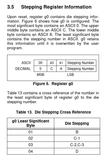
Fun game: try to find everything wrong with Figure 6.
Thanks to the work of one person that is thanklessly maintaining a GCC fork with i960 support over on GitHub, the software side of the project mostly focused on expanding my own C software libraries. I already had built up a little standard library for my RISC-V custom silicon, including a custom printf, some common C standard library functions, xorshift PRNG, software I²C driver and ext4 filesystem driver, so I mostly just expanded this what I needed for this board, which included the graphics and image decode functions (most ported straight from the i386 badge). Most of the work went into actually putting together the image slideshow shown by the badge. As planned, it does show the current time in the corner of the screen at all times, though interrupts on the i960 are weird and not something I managed to get to work cleanly, so instead, a timer is polled regularly to re-draw that portion of the screen. The pixel colors behind the clock are cached in memory to allow a fast transparency effect.
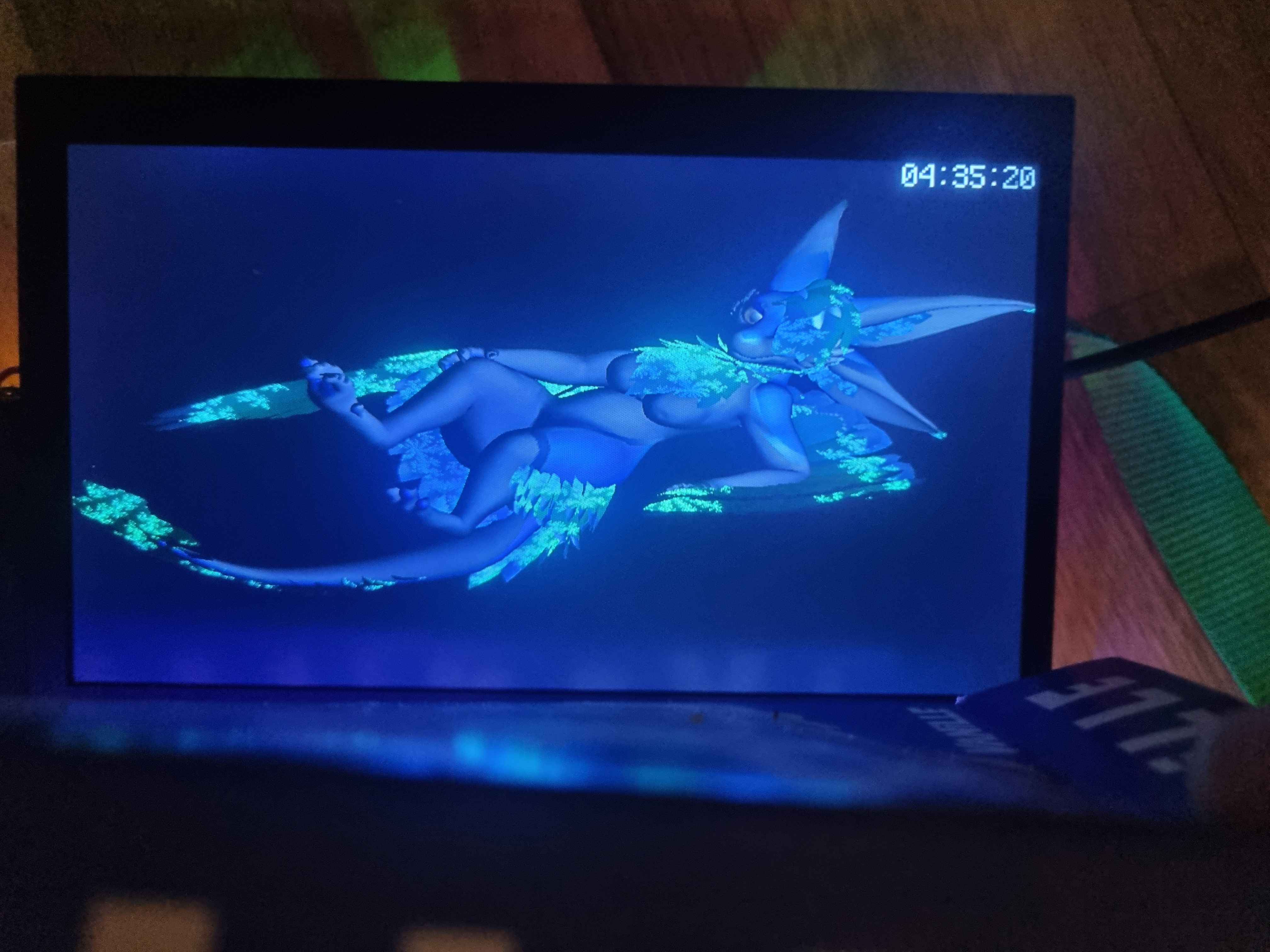
A few demos still made it in. A rule 110 simulation scrolls across all 600 lines of the screen at one point, and a Mandelbrot renderer can be tried by holding down a push button during certain parts of the slideshow. The 3D renderer has made a comback and is more impressive this time. I decided to use regular floating-point this time, as the fixed-point format caused artifacting on the i386. Though the version of the i960 I use, the "CA" variant, does not have hardware floating-point, so it is a bit slow. Still, I added pixel shader support on top of the lambertian diffuse lighting, so my wings render with the same shader effect they do in VRChat. Textures are also a thing now, though each material is limited to a single 512 by 512 pixel texture before running out of memory. Point-sampled. So there is some dirty tricks going on here, such as the fractal shader effect mask stealing a bit off of the red color chanel of the underlying texture. Note that the eyeballs have a transparent material with a specular highlight. I got this to the point where I can just port whatever shader code I already have, which is very good! The final render "only" takes 15 minutes too! And the CPU barely gets warm! Impressive!
The i386 badge page has some more info on the architecture of the filesystem driver and 3D renderer, so I won’t repeat myself here.
Issues?
Surprisingly, not many. Probably because using a FPGA as the chipset has the advantage that you can adjust it after manufacture. The only thing that really went wrong was a missing trace between a CPU output pin (BLAST) and a FPGA input, which I solved with my reliable "bodge wire with ground return" (a wire that has a another wire wrapped around it that is grounded on both sides). I finally managed to kill the EMI issues - by upgrading to expensive 6-layer PCBs and being more careful with my ground planes. The video board was actually my first 6-layer PCB, though it forced my hand with the complex routing requiring it, not EMI.
There might have been some remaining bus timing issues. After arriving at the con and powering up the badge for the first time, the bootloader failed repeatedly with a bad CRC error. But waiting for a minute or two for the system to "warm up", it went back to normal. But the result always was the same: flawless operation even after hours of uptime and the batteries running low. Though this is now two cents for a badge working perfectly on the bench for weeks and then trying to break on-location first day before going back to normal.
All in all, I think I have successfully managed to set a solid standard for what my custom badges should be. And it only took 4 years! This badge you program, turn on, and it JUST WORKS! Though this does mean that I’m not sure what to do next. I like the low power consumption of a RISC CPU, but am, as always, looking towards the horizon for more performance. Currently am looking into MIPS, but we’ll see. Video also is a big problem, though re-using the same video board is tempting.
In any case, everything related to this project can, as always, be found in my con badges repository.
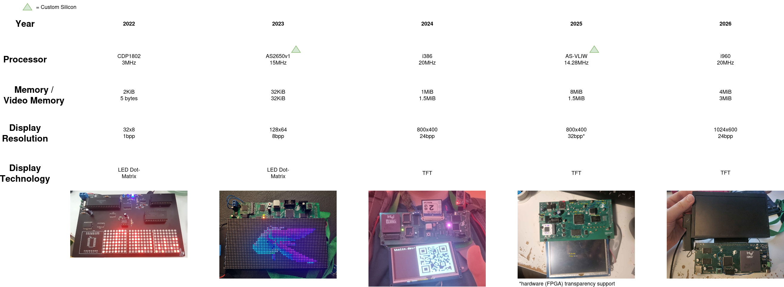
OH! And just to recap how far I’ve come, here’s a little infographic: