
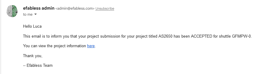
Custom Silicon Adventure (p.1)
If there is one thing that I really enjoy doing the most, it is building computers, as should be obvious by the content under this section of my site. Even after all these years, my fascination with computers has yet to fade. But of course, there is only so much I can get out of using other people’s CPU designs. I always want to peel back even more layers in computer design, do even the part of designing the CPU myself.
Infact, I’m not alone in that sentiment, if the number of entries on the Homebrew CPUs Webring is any indication. Actually, before I even built my first computer around a microprocessor, I attempted to use 74-series parts to DIY my own CPU. It wasn’t very good, and turned into a mess of wires. It did work, though so maybe one day, I will actually make a post about it on this site.
However, my true dream of building even the contents of the actual ICs myself is something that formed very early on in my adventures, thanks to Sam Zeloof, and his attempts to build his own ICs in a garage. Though of course, he has access to more tools and resources than I could ever dream of, and so my custom IC Ideas appeared doomed to remain a pipe dream forever.
And then, in October 2022, I heard about Tiny Tapeout for the first time.
Tiny Tapeout
Tiny Tapeout is a project created by Matt Venn to allow people to get simple chip designs fabbed for a very low price. When I originally found out about it, submissions were open for TinyTapeout 2, and the constraints for those early TinyTapeouts were high: you got 8 output ports, 8 input ports a tiny die area of 150µm by 170µm AND the clock speeds were limited to 10kHz.
Of course, I tried to design a CPU within those constraints. I called it the "AS5401". It is only 4-bit, but has a 12-bit Program Counter and 8-bit Memory Address Register, as well as facilities for hardware multiply and divide. Despite this, I still had die space left, which I filled with 10 words (5 bytes) of on-die RAM. And, all crammed into an ISA of just 16 opcodes.
I actually designed this CPU using Logisim Evolution, after I found a way to extract HDL netlists from a Logisim project, for using with TinyTapeout’s GitHub action workflows. I did this because I figured I wouldn’t have enough time to learn a whole HDL and I did design my 74-series CPU at the logic level, after all, so why not do so here?
I was done a lot faster than expected, gave myself a crash course in Verilog, and ended up gaining the record for most individual projects submitted to a TinyTapeout shuttle (I believe I still hold it as of me writing this). I even contributed back to TinyTapeout, helping with debugging the GitHub action pipelines as well as writing a guide for their website.
I won’t go into too much detail on my TinyTapeout projects, as they are not supposed to be the main focus of this post, but here is a list of all my submissions:
| Name | Description | GitHub Link |
|---|---|---|
| AS5401 | 4-bit CPU | AvalonSemiconductors/tt2-AvalonSemi-5401 |
| TT02 Logisim Example | Examples & Documentation on how to submit to TT using Logisim Evolution. | AvalonSemiconductors/tt02-logisim-example |
| Diceroll | Animates a random number rolling on a 7-segment display. | AvalonSemiconductors/tt2-diceroll |
| TBB143 | Programmable Sound Generator using a ring osc as a faster, internal clock. | AvalonSemiconductors/tt2-avalonsemi-TBB1143 |
| Multiplexed Counter | Multiplexes 4 7-seg displays to count time up to 99 mins, 59 secs. | AvalonSemiconductors/tt2-multiplexed-counter |
| 4-bit multiplier | Multiplies two 4-bit numbers to 8-bit result. | AvalonSemiconductors/tt2-4x4-multiply |
| LCD Namebadge | Experiment with interfacing a character LCD. | AvalonSemiconductors/tt2-lcd-namebadge |
It was at this point that I set up a organization account on GitHub named "Avalon Semiconductors", because the amount of repos just for chip designs became a bit overwhelming and needed its own corner on the internet, which also lead to me adopting the prefix "AS" for future chip designs.
I also submitted to the unofficial "TinyTapeout 3.5", a shuttle which was supposed to test a new fabric for wiring up all the designs on the chip. I submitted a replica of the CDP1802, with some new instructions and peripherals added, though this didn’t happen until after the rest of the adventure I’m about to explain.
Efabless & OpenMPW
Of course, TinyTapeout doesn’t exist in a vacuum. Some fab has to build the actual chips for them, but for TinyTapeout itself to have a direct contract with a fab would be difficult to impossible. Instead, Efabless is the company responsible for handling not just the logistics of getting the fab done, but also includes packaging of the chips, and provides all the software and hardware required to design and test your chips in the first place.
OpenLane is the tool they have built for automatically generating the hardware circuits and design files for a chip from a Hardware Description Language. It is even Open-Source. Skywater Foundries is the fab Efabless has chosen to work with, specifically their 130nm process node, the development kit for which has also been open-sourced.
Efabless then organizes quarterly multi-project wafer shuttles to be sent for fabrication. Every one holds 40 slots for individual projects to be fabbed, and TinyTapeout is just one of them. TinyTapeout then further subdivides this space to its participants to drop costs even further.
Submitting to a shuttle like that would, of course, be the dream for me. Because, lets face it, designing a IC under TinyTapeout 2’s constraints was still far from my original dream of building my own microprocessor and having it be something useful. Unfortunately, this service costs at least 10 grand. Incredibly cheap relatively speaking, but way more than someone earning minimum wage could afford. However, at the time, there was OpenMPW.
The now-defunct OpenMPW series of shuttles was intended for anyone to get their first experience building more complex integrated circuits, and also ended up being quite a useful stress test for Efabless’ tooling. Essentially, every quarter, there would be a "free shuttle" running in parallel to the regular, paid one, where anyone could get a slot for no cost at all. Of course, there was always more than 40 people wanting a free seat, and so of the submitted designs, 40 were randomly chosen for fabrication.
GFMPW-0 was one such shuttle (and one of the last), which would not be taped out on Skywater 130nm as usual, but instead aimed to try Global Foundries 180nm process. By the time I learned of it, the submission deadline was less then 14 days away. Still, I was dead set on creating a submision to it, meaning I had to come up with a goal I could meet in just under two weeks.
Designing the AS2650
I very quickly settled on re-creating an existing design, rather than trying to come up with something of my own within the limited time frame. And of course, with me having been quite obsessed with the Signetics 2650 lately, the choice was obvious. The original goal was this: re-create the architecture of the AS2650 1:1 first, minus that weird memory paging system. Then, make use of the unused opcodes of the 2650 to implement custom functionality on top. And, finally allow the internal stack to spill over into memory. (For more information about the 2650 itself, see my dedicated page for it.)
I ended up not meeting any of these goals to 100%, despite sacrificing every second I was awake for the next two weeks.
I certainly believe I could do it now, but at the time I was still not very comfortable in Verilog, and struggled a lot with doing verification. Actually knowing what I wanted and how to do it weren’t as much of a problem as expressing it in Verilog. As stated earlier, I had plenty of experience doing logic design at the gate level, but it ended up helping me little when working on my first major project in Verilog.
The thing that I spent the most time doing is staring at GTKWave traces, trying to figure out why some instruction was not executing correctly, only for the actual problem to end up being some minor mistake.
A note on CPU design at this point. The way one usually designs a CPU is actually like a state machine. It begins with some form of instruction fetch, followed by a decode, and ends with any amount of execute stages before looping back to the begining. Every clock cycle, the state machine advances forward by one state. Because of this, you usually want to minimize the number the number of execute steps.
This was actually one of the improvement I made over the original 2650, which actually split every state machine step into a read-modify-write cycle taking 3 clocks each. Instructions could take as long 12 clocks. Of course, I was way less constrained using a "modern" CMOS process on a almost 10mm die area, and reduced each instruction to the minimum number of steps required. This modernization of the 2650 design was how I intended to gain the majority of extra performance. Infact, all I had for reference was the 2650’s datasheet, which I was constantly referencing and re-reading. My chip design was only similar to the original in that it was going to be backwards-compatible in bytecode (that was the Idea, at least).
However, of note is the instruction decode step. Unlike the other steps in the state machine, this one is actually implemented purely in combinatorial logic and if done right, may not even take a whole clock cycle to execute, and so happens asynchronously between the fetch cycle and the first execute step. This is something I managed with the AS2650 (though kinda unintentionally), but it lead to me writing quite a lot of spaghetti code, evaluating complex expressions directly in conditional statements without re-using or naming any of these expressions. In general, my code ended up becoming a huge mess of nested if and end else if with little code re-use. This I blame more on the (kinda unfair) time crunch than my own inexperience. Remember this spaghetti code. It’ll come back to cause me a lot of pain later.
By the time I had finished implementing the base ISA of the 2650 (except the extended IO instructions, which I dropped), I was running extremely low on time. I still wanted to run further verification and add some custom instructions to the architecture. I did end up doing a bit of both, though to very limited degrees. Some instructions on the architecture went completely unverified, and I only added 4 new instructions to the architecture:
| Mnemonic | Description |
|---|---|
push
|
Pushes r1, r0 onto internal stack. |
pop
|
Pops from internal stack into r1, r0. |
xchg
|
Exchanges r0 and r1. |
mul
|
Multiplies r0 by r1, 16-bit result in r2, r3. |
push and pop are what is left of the Idea of having the internal stack spill into RAM. I also wanted to have hardware multiply and divide, but ended up with only multiply. The multiplication is single-cycle, though.
There are other CPU features I had to drop as well, such as interrupts. Those were a bit weird on the original 2650, so I was going to come up with my own interrupt logic. I also dropped the OPACK pin, which can be used to make the CPU wait on memory accesses. As stated earlier, I omitted the original memory paging mechanism, but never even came up with a better replacement for it. As a result, the AS2650 is permanently stuck only being able to address 8192 bytes of memory on its own.
At this point, the clock was quickly ticking down to zero. But I decided to be confident about my creation and went on Efabless’ website to make my submission. This involved running a final set of DRC checks on your design, before running the Tapeout job to generate the final production files. Then followed a nervous wait for the lottery balls to fall into place, and...
It was more like a coin toss (84 projects on a 40 slot shuttle) than a lottery, but this was still the most exciting news I had gotten all year (and it was december!). Unfortunately, it was to be followed by a long wait. Efabless projected a 6 month long wait for Global Foundries to finish the wafers and for someone still my age, that is basically an eternity. So, in the meantime, I should explain a few more things that will be important to the story.
OpenLane
At this point, I’ve only explained how I’ve designed my chip on paper and in Verilog. But I’ve yet to explain how to actually get a chip design out of that in a format that the fab will understand. And its easy, really.
There is a repository that you clone called caravel_user_project. There is a Makefile to make setup to download all the tooling, and then you drop in your RTL Verilog, making sure to instantiate your design in the included top-level module. There is some config files involved as well, but you’re fine just re-naming the ones from the included example project. Then, you’re ready to run make [your project name] to run OpenLane to generate the GDSII file (like a gerber file, but for silicon instead of PCBs). make user_project_wrapper will then build the whole user area GDSII with your design in it.
If that sounded like I am oversimplifying and skipping a thousand extra steps, I am really not! If there is one I think I couldn’t blame for any issues in my design, its the tooling. For just creating a simple design entirely in Verilog, the process is incredibly streamlined. OpenLane and the target fab’s Process Development Kit are installed for you, and everything else is neatly wrapped in docker images. There are, of course, a couple config options you may need to play with, such as the Verilog includes, macro size and target density. And things may get a bit more complex when working on a design built out of multiple macros, or including analog components. But I did spend most my time actually working on my design, rather than struggling against the tooling.
Standard cell sky130_fd_sc_hd__dfxtp, implementing a D-Flip-Flop.
All of this is because of the amazing OpenLane tool I mentioned earlier, which does all of the heavy lifting for you. If you’ve worked with FPGAs before, you may already be familiar with similar flow tools used to generate a whole FPGA config for you. OpenLane is that, but for ASICs, which is quite a step higher in complexity. Instead of setting up and connecting logic cells, it has the difficult job of generating actual circuitry. This is of course simplified through the use of standard cells supplied by the fab. A standard cell is a very small bit of circuitry implementing a simple logic function, like a logic gate, flip-flop or full adder. These are what are placed and routed by OpenLane, even designs with tens of thousands of these cells.
OpenLane will also run various timing analysis for you and let you know if things aren’t working out for your desired clock speed. According to that, the AS2650 should be good at at least 40MHz!
Caravel
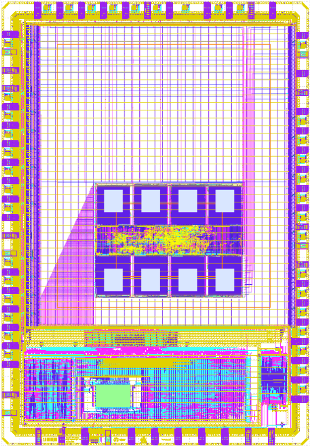
Another major thing of note is that any design submitted to Efabless will not exist in a vacuum. It’ll placed inside a wrapper called Caravel. Seen here is a visualization of a GDSII file for a Efabless chip. The user’s project is placed in the big area in the middle, with the Caravel surrounding it. At the bottom is a whole RISC-V (RV32I) microcontroller, called the management (mgmt) controller. It executes code from an external flash, and has access to a wishbone bus (a debug interface) and a series of logic analyzer probes, allowing on-chip debugging.
Also of note is that the user project is never directly connected to pads on the chip. Instead, every user-accessible I/O pin is routed through a configurable buffer. As the direction and purpose of each pin may be different depending on the user design, each buffer can be configured for a variety of modes. For instance, it may be a simple output, or an input with a pull-up resistor, or bi-directional or it can even be configured to be an analog pin, which does bridge a straight connection from the pad to the user design.
These buffers are hooked into the mgmt controller as well. It can monitor them or override the state of their signals, to generate test inputs to the user design and test its response. There is also a mode in which the mgmt controller takes over a pin, disconnecting it from the user design entirely and turning it into a GPIO pin for itself.
A register in each buffer determines its configuration, and the collection of all buffer register values is called the IO config, which can be written by the mgmt controller. However, using the mgmt controller is optional, and the user can supply a custom power-up IO config.
Bring-Up
I actually somehow managed to forget about GFMPW-0 for a bit, so it came as quite an exciting surprise when Efabless streamed a live seminar in which they explained that they not only held samples of GFMPW-0 chips in their hands, but the Caravel on them was fully functional. This was a massive relief, as the early OpenMPW shuttles were plagued by problems in the Caravel that went as far as making it difficult to even access the user designs inside.
However, now that it was clear that my design was going to be accessible, I had to start preparing for bringing it up. Efabless projected shipment of the assembled chips in two weeks, so I once again found myself in a rush (its starting to become a theme). It did end up being a bit longer than two weeks, and the shipping itself took its time, so I was able to have a custom bring-up PCB ready just in time.
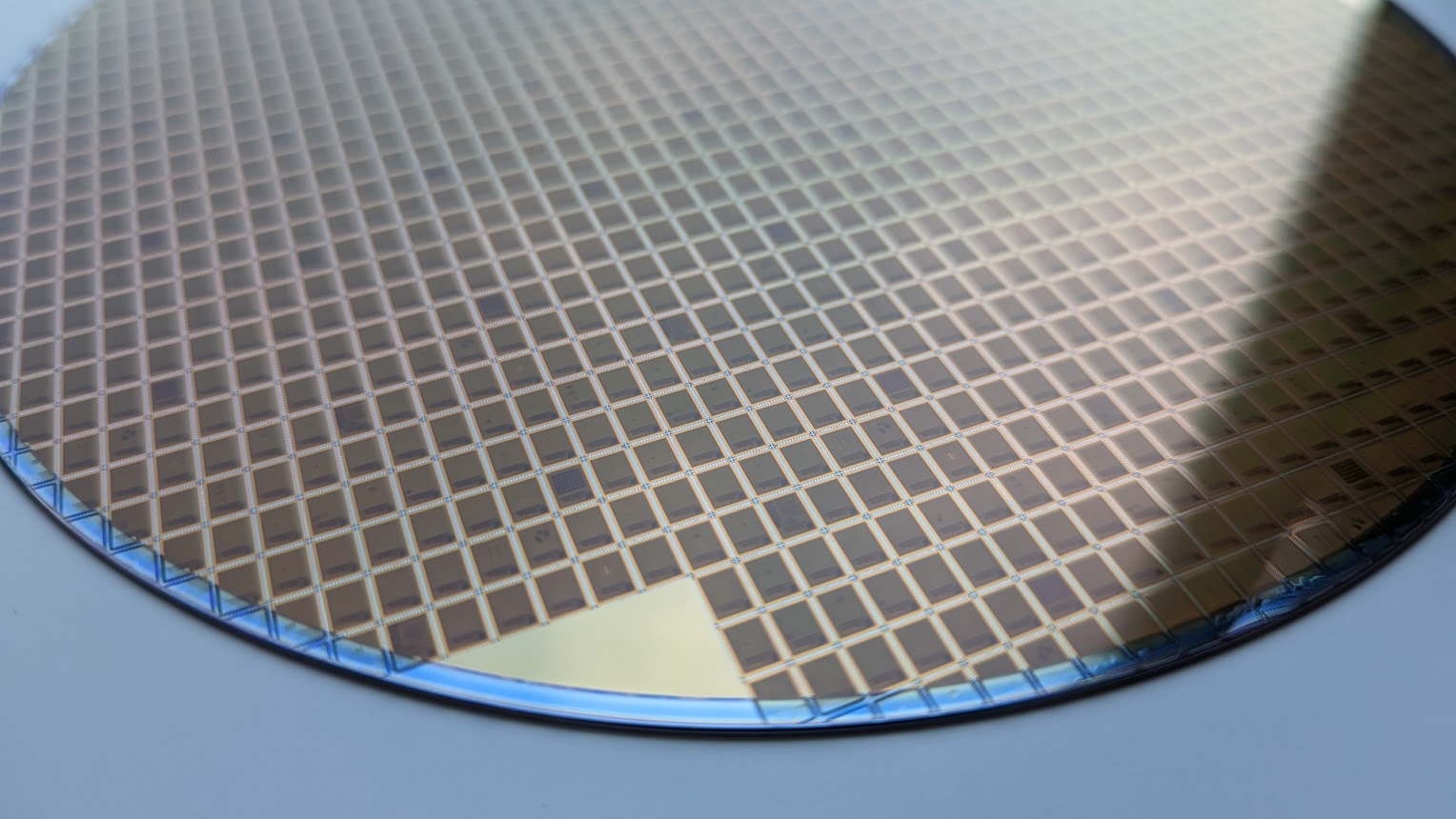
While I was waiting for that, Matt and someone going by the nick of Anish actually got their hands on raw GFMPW-0 wafers! I managed to reverse the placement pattern of the 40 projects on it to locate an instance of my design, and kindly asked Matt for a close-up. I’ve overlayed the dieshot with the GDSII render I submitted, though not much can be seen. Of the multiple metal interconnect layers on the chip, all but the topmost one have any unused sections filled-in, making them completely opaque. Only the power grid and topmost wiring can be seen.
I even took three days off work on the date the package was supposed to arrive, just so I could wholy focus on the bring-up.
And then, finally:
The package I received was quite small, but contained a lot. On top of the 10 chips pre-soldered to breakout boards, there were three tubes containing a total of 100 parts! I never thought I’d collect 100 of any active component, much less one I designed myself. Efabless even included two boards that a breakout board could be sloted into, to test the chip on it. However, I would only briefly use these, as I still had my own bring-up setup prepared.
However, first, I needed to do two things. Test the caravel management controller, easily done by making it blink an LED, then set up my CPU in a simple NOP-Tester configuration. Normally this involves using resistors on the data bus lines to hard wire a no-op instruction, then seeing if the address bus bits all count up.
In my case though, I could do most of this in the IO config, by configuring the data bus lines’ internal pull-ups to either be pull-up or pull-down. Then, I used the incredibly scientific instrument of a small speaker to test the address lines.
Hearing that square wave tone that doubled in frequency as I moved the probe down the address lines was definitely a heart rate doubling moment. My CPU was indeed alive in there, trying to find code to execute, which meant the moment of truth was rapidly approaching. So, its time to finally reveal what was my solution for bringing it up.
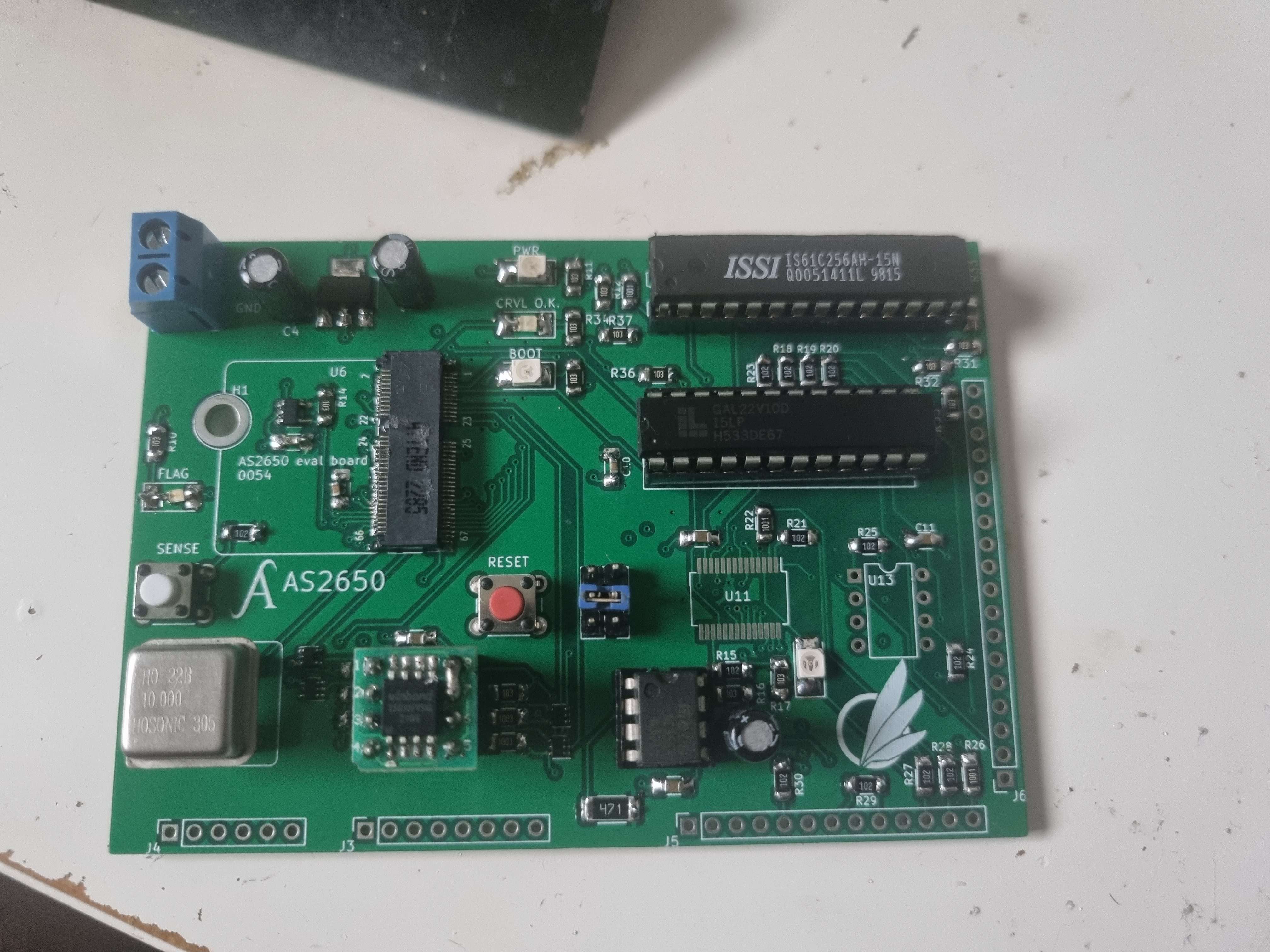
This small board features all the components for a minimal system with my CPU, plus some peripherals. I didn’t even fully assemble it at first, wanting to wait until I knew my design wasn’t totally broken. So far, it features a slot for the break-out board, a flash ROM for the mgmt controller, a 32KiB SRAM IC (of which only 8KiB would be used) and a GAL (Generic Array Logic) for glue logic and basic I/O. Also, the can oscillator is socketed, so I can play with the clock speed.
As may be evident, these parts were not my first choice. My original Idea involved a CPLD and a RAM chip that wasn’t older than me, but Global Foundries threw a wrench into those plans. Their 180nm process requires a 5V supply, as opposed to the 3.3V Skywater 130nm process. I wanted to have a board design I could be confindent in for the bring-up, and so I did not want to rush engineering a solution with too many parts, such as level shifters. This lead me to the 61C256, a SRAM IC used for external cache on old CPUs such as the i386, and a 22V10 GAL, a very early kind of programmable logic device.
The GAL is just barely complex enough to not only generate the control signals for the RAM, but also respond to I/O bus cycles from my CPU to provide it with 5 output ports and a single input port. I was intending to bit-bang some SPI devices through these ports later on.
The PCB contains some hardware bug workarounds as well! While waiting for the chips to arrive, I already identified some problems. Relevant for now is that the power-up IO config for the Caravel was wrong! Instead of exposing my design straight away, some of the pins would be connected to the mgmt controller. Luckily, this can be fixed by the mgmt controller itself, by writing a new IO config. However, this is where the second issue comes in. It is usually good practice to have the user design have a separate reset pin, using one of the user IO pins. Of course, I decided to just use the convenient wb_rst_i input in the Verilog code, tying my CPU’s reset to that of the mgmt controller.
Essentially, I cannot re-write the IO config while holding my CPU in reset, meaning it’ll be in some unpredictable state once its pins finally get connected properly. The solution would be to use gpio, a pin on the chip exclusively owned by the mgmt controller, to trigger the chip’s own reset. A magic value in a magic memory location would indicate to the mgmt controller firmware if it had already reset itself, to prevent a infinite loop.
A 555 timer was supposed to stretch the reset signal, but of course, of all the things for me to mess up, it had to be the simplest. I got the polarity of the 555’s trigger wrong. I ended up bodging gpio directly to reset, which worked for now, but would cause issues later.
The first bit of code ever executed on a AS2650
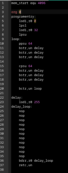
Finally, popping in my IC, it was ready to run its first program. There is no ROM on the 8-bit data bus of the CPU, but that would be no problem. May as well make use of the mgmt controller’s ability to take over the IO pins, and use its firmware to write bytecode into RAM before the self-reset.
Of course, the first program to try and run had to be an LED blinker using the built-in Flag output. After struggling with the mgmt controller firmware quite a bit (it appears to have an issue where 8-bit loads from flash can lock up the microcontroller core), it was finally time for my CPU to execute its first bit of actual code! Aaaand it didn’t appear to work! The LED turned on and stayed like that. Panicing a bit, I realized the loop may be going too fast, so I once again made use of the speaker to hear the Flag output, which revealed a perfectly, though quickly oscillating signal. I had breathed actual life into my design for the first time!
Of course there was much to be done still, but only after a celebratory break ;)
The next order of business was to test wether my CPU can write to RAM as well, and then to try and blink an LED on the IOs provided by the GAL. But it was actually smooth sailing at this point, with the most suspenseful parts behind me. At this point I also finished assembling the PCB, giving it its SPI peripherals: a port expander usually used with Arduinos, providing me with 16 individually programmable GPIO lines, as well as a second SPI flash.
The first thing to do, of course, was to flash an LED on the port expander. I find it amusing how this whole bring-up process just involved increasingly elaborate ways to blink an LED. But that was about to change.
I was getting quite tired of having to re-compile and re-flash the mgmt controller firmware each time I wanted my CPU to run a different program. So I developed a bootloader, which would be the thing initially in RAM, and would always be the same. It loads the actual program off of the flash on the bitbanged SPI port.
I also wanted a UART, and instead of inventing something new, I used the same UART module I developed for my Signetics 2650 computer and which I’ve sinced used in many such projects. Of course, the bus speeds of the AS2650 are too high for it, so the true purpose of the port expander is it to talk to the P8251 on that module. It’s a lot of hoops to jump through, and a bit slow, but it gets me a simple dev console.
The only issue is that the P8251 sometimes doesn’t reset properly. Evidently, without the 555, the reset pulse is too short for it.
But, everything appeared to be working so far, and I was ready to execute some more complex programs.
Almost-final look of the bring-up board. The bodge wire ended up being temporary.
Silicon Bugs are the worst
Unfortunately, it was not to be for now. Of course, when you throw together a chip design in two weeks, its not going to be perfect. I was already aware of this, having identified one broken instruction ahead of time. Relative addresses indirect branch instructions would not execute correctly, which is a minor issue, actually. The workaround is it to just always use absolute addressing as the base addressing mode of these instructions, so I didn’t pay it much mind (though it did make me sad that binary compatibility with the Signetics 2650 was now broken).
But I really should’ve seen it as an omen of what was to come.
You can go read the full bug list over on my GitHub, but there is only one on there that really killed my excitement for my own project, at least for a while. Both addition and subtraction with carry are broken in a major way. I first noticed this trying to run my mandelbrot set renderer program from the original Signetics 2650 on my bring-up board, but it came out looking very weird, and it took me almost a whole day to trace the problem, partly because of my own denial that I could’ve messed up that badly.
psl[0] <= alu_next < input1; is the problematic line in my Verilog. Even for a rushed project, that is pretty bad. Another thing I’d probably attribute to my gate-level logic design skills poorly translating to Verilog code. Still, I can barely believe I was actually sober when I wrote this.
Now, why was none of this caught in verification? Usually, a lot of code goes into verifying every single CPU instruction on every possible scenario. That is where that time crunch rears its ugly head again! I was infact aware of this way of doing verification, because its what I did for my 4-bit CPU for TinyTapeout 2.
But not only was I in a rush for GFMPW-0, but the verification framework that is usually included with the caravel_user_project repository was not ready yet for Global Foundries 180nm. I had to throw something together myself the only way I knew how, and had to forgo gate-level tests (where every standard cell in the final flow netlist is individually modelled).
My testing method ultimately consisted of bringing up the CPU in simulation, and letting it run a test program stored in a simulated block of RAM. At the conclusion, the test runner would check if the RAM was in a specific state. Not only did this distract me from testing all possible scenarios, I didn’t even have time to include some instructions in the test program (such as the broken push).
The frustrating thing is how close I came to discovering the issue in the ALU. I was going to take that mandelbrot renderer program and run it in simulation as a final test, but just barely did not have enough time. I absolutely would’ve discovered this issue before the deadline otherwise. Though there are also bugs I had no hope of catching like this. For instance, the return from subroutine instruction takes 256 clock cycles to execute, but still technically works after those have elapsed. I even use it plenty within my existing verification, but at no point does it count instruction clock cycles. It only cares that they have the correct effect.
There is a workaround to the ALU bug, as with the other bugs, but it is ugly. A 7 instruction long sequence must surround any add-with-carry or subtract-with-carry that specifically checks for the condition causing the bug and forces the correct result.
I was able to render my mandelbrot set correctly in the end, but the code for it is indeed quite ugly now. It also frustrates me to no end that my CPU cannot to arithmetic correctly.
The clock speed of the CPU is also severely constrained not by a bug, but a lack of foresight on my part. By omitting the OPACK pin, which can be used to make the CPU wait on slower memory accesses, I’ve forced a condition where every memory or IO request must be served within a clock cycle. The fastest I was ever able to push the clock on the AS2650 was 27MHz before the latencies got too long. And a overvolt to 5.4V was required to get the computer to be stable at the 25MHz I usually run it at.
I am thermally limited in this regard as well. At 25MHz, the chip already gets hot to the touch to the point where I attached a small heatsink to it before I was comfortable continuing to run it at that speed. I asked some other GFMPW-0 participants about their chip temperatures, but I appear to be the only one with this particular problem.
Ultimately, I am not too upset about this, though. 25MHz is, I believe, still a respectable speed for an 8-bit microprocessor of this type, and still a 25-times speed-up over the original Signetics 2650 before even considering the improvements I made to the IPC.
AS2650 Con Badge
After the semi-successful bring-up, it was now time to use the AS2650 in an actual project. And what better way to do that then to build myself a successor to the CDP1802 badge. After all, taping out your first custom IC does earn you some bragging rights.
This time, the board is a bit better engineered, finally using level shifters to allow me to embed a MAX II CPLD. It mainly handles driving the LED panel using a separate SRAM to contain the framebuffers. The CPU can ask the CPLD to write into those buffers in-between pixels being shifted out to the screen.
There is also a timer in CPLD, though the CPU has to poll it to know when a frametime (1/20th a second) has ellapsed. Remember that the AS2650 has no interrupts. A SPI bus is also handled by the CPLD to talk to a SPI flash. There is even a connector for a NES style controller on the board, also driven by the CPLD! I am using up all 240 available logic cells in the CPLD for all that. I paid for the whole CPLD, I’m gonna use the whole CPLD!
Other than that, its a similar setup to before, with the mandatory mgmt controller flash, and 32KiB SRAM for the AS2650. This time, all 32KiB are accessible through a page swapping system implemented by the CPLD as well.
Unfortunately, clock speed is even more constrained here. I tried to get the fastest level shifters I could, but there is a critical path during IO reads that goes through both level shifters and the CPLD. Even at 15MHz, the board is a bit unstable unless I once again overvolt slightly.
As for what the badge does, it starts off with a bit of info about me, but quickly descends into a series of demos ranging from drawing lines to rendering 3D graphics! I went through the effort of implementing a 3D rasterizer renderer using a depth buffer to solve occlusion. At the end of the video, you see the badge rendering a 1500 polygon model in just 90 seconds. The code for this is only 2000 lines of assembly as well.
Conclusion?
Far from it! As I said at the very begining, I’ve dreamed of designing my own microprocessor, and that still holds true. The AS2650 was a re-implementation of an existing design. One I am a huge fan off, of course, but not one I created myself. I was going to create custom instruction extensions to it to make it feel more like my own, but that ended up mostly falling flat due to time constraints (one of the instructions I added doesn’t even work!).
On top of that, I was still using the automated flow tools. I already tried drawing a inverter and NAND gate by hand in Magic, and it got me itching to try designing something in the analog domain by hand.
Lastly, I absolutely hate seeing a project with as many issues as the AS2650 go without a revision 2. I always look at those chips and feel a deep need to fix things. On top of that, I always notice all that empty space in the GDSII renders of my submission. So much blank space that I could’ve done fun things with, given more time. On chip RAM? Built-in peripherals for IO, graphics, and sound? A second CPU core?
In another time, this would be where I would have to call this journey over. Funding for the OpenMPW shuttles dried up at Efabless after GFMPW-0 and $10K for a spot on a paid shuttle is going to be impossible for me for a long time. And TinyTapeout, despite their continuous improvements, just cannot contain my ideas anymore.
But, fate would not have it. As it turns out, I would get a chance to make the AS2650 of my dreams, and so much more.
Repos & Sources
The sources for this project are spread over multiple repos, as listed below. I’ve done my best to fix all the bugs in the source Verilog of the AS2650 in the "AS2650" repository (other repos intentionally contain still bugged Verilog for accurate simulation), so it should be usable on something like an FPGA.
| Description | Link |
|---|---|
GFMPW-0 submission repo - last v1 commit
|
AvalonSemiconductors/AS2650 |
AS2650 bring-up board hardware, firmware and software and custom assembler
|
AvalonSemiconductors/AS2650-bring-up |
AS2650 Con Badge hardware, firmware and software
|
89Mods/AS2650-con-badge |
You may also want to read my post on the original Signetics 2650 or check out its repo containing hardware and software for the original 2650.
Acknowledgements
Efabless and Global Foundries for providing me with this opportunity
Matt Venn for creating Tiny Tapeout, setting me on this path, and being kind and patient with all my questions when it came to OpenMPW.
The original Signetics 2650 design team for inventing something awesome.