
Signetics 2650 Microcomputer
Of all my microcomputer builds, this one is probably the most unique. It features a CPU that I stumbled accross quite by accident: the Signetics 2650. Its a very obscure chip, only used in some low-cost video game consoles in europe, despite Signetics’s heavy marketing of the processor. It only saw a limited production run, meaning finding one is quite hard, but after months of watching eBay, I finally managed to obtain one.
The 2650’s obscurity is what actually drew me towards it. I enjoyed the Idea of being one of a limited amount of people to have ever used one, as well as hopefully documenting as much about it as I could, to help preserve its existence. So, this is gonna be a long one. I plan to not leave out any details in documenting this CPU, its architecture, and the computer I built with it.
CPU Architecture
Pinout of the 2650. Source.
The 2650 comes in a DIP-40 package, similar to most 8-bit microprocessors. It has the usual address and data buses, R/W, interrupt and run/bus enable pins, as well as some response signals for those. "Sense" and "Flag" are unique, with Flag being a general-purpose output, and Sense being an input.
However, one may notice that there are only 15 address lines, not 16. And that is indeed correct. The 2650 can only address up to 32KB of memory. Of note is that A13 and A14 are multiplexed with the I/O bus control signals. The 2650 has two types I/O instructions: simple and extended. Simple only has a single "address" output for it (D/C). The intended way to use it is to have a latch respond to one of them, so an I/O address can be latched externally. However, it can also be used as a simple 1-bit address to switch between two devices, which is what I ended up doing.
Extended outputs two bytes: one on the address bus, and one on the data bus, to instantly send or receive a byte from one of 256 I/O addresses.
The actual instruction set architecture was supposedly inspired by the IBM 1130 minicomputer, but its barely recognizeable as such. There is a total of 4 directly accessible general-purpose registers on the chip, simply labeled r0 - r3. However, r1 - r3 are banked, and can be instantly swapped for an alternative set, yielding a total of 7 registers.
The CPU does not have a specific accumulator register. Instead, arithmetic and logical operations can be performed on any of the visible registers directly. However, a special function is given to r0 in the form of its own addressing mode.
A zero-addressed instruction will always operate on r0, and another register, for instance, adding r3 onto r0, or storing r0 in r2. This ability to do register-to-register operation is indeed incredibly useful, as it allows programming entire algorithms without accessing RAM.
All registers can also act as index registers. Any instruction that accesses memory can have the value of one of the registers added to its effective address. The register can also optionally be incremented or decremented before the operation. This allows constructing one or more data stacks using any register as a stack pointer. As a result, the 2650 does not have a dedicated stack pointer register for stacks in memory.
All branch instructions in the 2650 are conditional. The CPU stores a 2-bit Condition Code (CC) after certain instructions, and branch instructions can be set to only trigger if this code is equal, or not equal, to a certain value. As the CC will never be equal to 11b, a instruction with this condition will be interpreted as unconditional. The meaning of the contents of the CC changes depending on the instruction that generated it, but a comparison between two values is usually involved, with the CC then indicating a status of greater-then, equal or less-then.
One interesting aspect of the 2650 is its integration of some two’s-complement, signed byte operations. The compare instruction will actually compare its two operands as signed values (arithmetic comparison) by default, with a setting needing to be changed to make it do logical (unsigned) comparison instead.
All of the status codes and settings of the CPU are accessible through the program status word, which is comprised of two registers, PSU (program status upper) and PSL (program status lower). Upper contains the state of the Sense input and Flag output, the Interrupt Inhibit bit and a 3 bit stack pointer (more on that in a moment).
PSL contains the CC, Interdigit Carry (for BCD arithmetic), Register bank select, Overflow bit and Carry bit. It also has two bits that change CPU behavior. WC determines if the rotate left/right, add and subtract instructions will use the carry bit, and COM changes the behavior of the compare instruction between arithmetic and logical comparison.
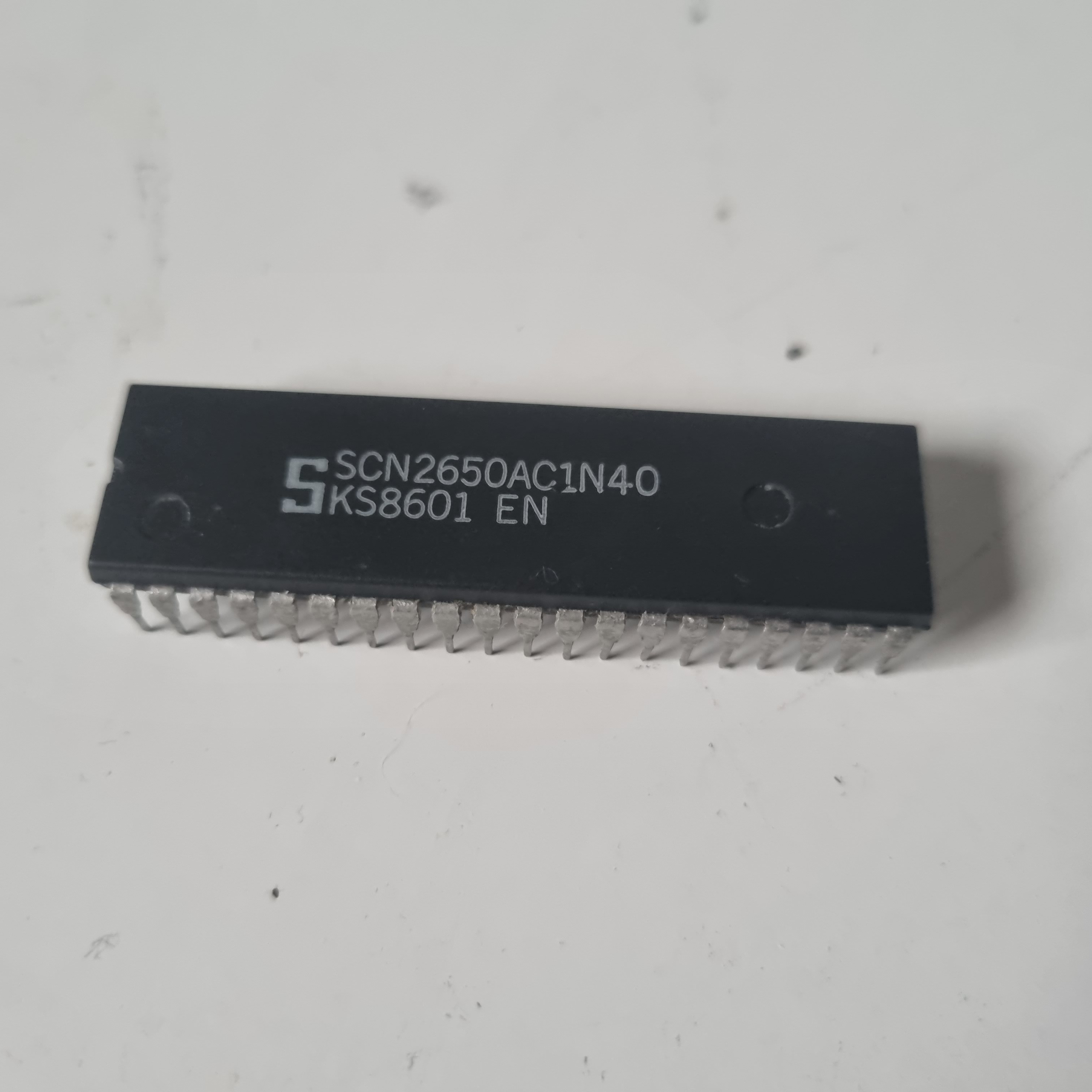
The S2650 I own.
Subroutine calls on the 2650 work a bit strangely. Instead of using a stack in memory, a 8-level deep stack on the CPU itself is used. This entirely removes the need for RAM to store a call stack, but also cripples the CPU a little bit, as the stack cannot spill over into RAM. 8 subroutine calls is as deep as you can go, and you’ve hit rock bottom. Luckily, this isn’t too bad a limitation for most programs. Because branch instructions support indirect addressing, it is also feasible to construct a call stack in RAM in software, if you really have to.
Lastly, however, there is one feature of the 2650 which I absolutely despise, and that is its odd memory access pattern. The CPU splits its 32K address range into 4 8K pages, and the way they are accessed is...stupid. By default, you can only access the page that program execution currently resides in. Basically, the most significant two bits of the program counter are equal to the current page that memory accesses happen in. If you want to read some data from page 1 while executing in page 0? You have only two options. Branch program execution into that page, retrieve the data, and branch back (doable through a block of RAM that is accessible no matter the current page), or use indirect addressed instruction, which is slow (6 additional clock cycles).
Neither of those are really options, or easy to work with. As a result, I ended up not bothering, and treating the CPU as if its entire addressing range was only 8KB.
Clearly I wasn’t the only person who disliked this system, as it ended up being contributor to the chip’s commercial failure.
Though in the end, I can understand why this was done. In order to allow indexing and indirect addressing in the instruction encoding, sacrifices had to be made when encoding memory addresses into instruction arguments. And as a result, memory had to be paged.
All in all, the 2650’s architecture can best be described as halfway between the 6502 and Z80 in complexity. Its a nice balance, in my opinion, and its definitely the architecture I’ve had the most fun writing code for.
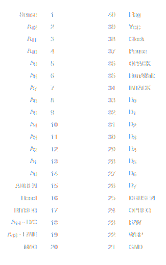
Instruction set
Instruction matrix for the 2650. Click to view. Source.
Generally speaking, the CPU’s instructions can be split into one of a few categories. Load/Store, Arithmetic, logical, comparison, branches, I/O instructions, instructions to access the program status word and three miscelanious ones.
Most of these are what you’d expect on a 8-bit processor. Add, substract (with or without carry) and the logical operations of OR, XOR and AND are all implemented. Branches to go somewhere else, as well as subroutine calls and returns.
The instruction mnemonics are unique, though. I always hated how 6502 assembly used magic characters to indicate addressing modes. You had to remember if a dollar sign meant immediate or absolute. Here, its part of the instruction name. loda means load absolute, and addi means add immediate. Its a lot easier to remember. Instructions that operate on a register have that indicated by a ,rx attached to the opcode, which is also a lot more explicit. I always find code written for the 2650 to be very easy to read.
As for addressing modes, there are 4 for all arithmetic and load/store instructions. Immediate, operating on the instruction argument, absolute, operating on a value from any memory address, zero, operating on r0, and relative. Relative is a bit useless, though, as it uses a signed 7 bit value as its argument, indicating a displacement relative to the instruction. I like separating my code and data sections, and so never find myself in a scenario where my data is close enough to my code for this addressing mode to work. It is technically faster, but not by much, and only useful for loading constant data when running in ROM, so not a big loss for me.
There is also indexed and indirect modes, but those can actually be added on top of the relative or absolute addressing modes, rather then being modes of their own. Indirect will read two bytes from the address pointed to by the instruction and use that as the effective address. Indexed will add a register’s value on top of the effective address, with the option to increment or decrement the register value before the operation.
Indexed and indirect can even be used at the same time, leading to the most complex instruction the CPU can execute: adda,r0 *address,r2+, which will load two bytes from address, increment r2, then add r2 onto the address, load from there, and add the value onto r0.
Of note is that indexed addressing can only be used if the destination register is r0, and adding the register value onto the address is always the last step in address calculation.
Branches can either be absolute, or relative. Relative also uses a 7-bit signed value as the displacement, and here, it is actually a useful addressing mode, particularly for small loops. Indexed addressing cannot be used here, but indirect can, in which case the branch destination is read from memory. Subroutine calls are the same. All branches, subroutine calls and even subroutine returns are conditional, with one of 4 conditions: equal, greater-then, less-then and simply unconditional. Wether a instruction will branch depends on the value of the Condition Code, as described earlier.
Lastly, there are instructions for modifying or reading the program status word, and I/O instructions, which read or write a register value to an I/O port.
However, there is more. Undocumented instructions are a thing here, and of course, I tried executing them despite the datasheet telling me not to. Unsurprisingly, two of them are duplicates of existing instructions, and most of the rest of them are nops. However, 10h and 11h do actually cause undefined behaviour. I’ve seen them clear or set random bits in registers r0 or r1, or also randomly do nothing.
The instructions labeled nopi are the more interesting ones. They reside in the same column as the immediate-addressed instructions, and the same row as the store instructions. However, "store immediate" isn’t exactly a thing, so these do nothing. Strangely enough, however, the processor does recognize them as being immediate addressed, and they will cause it to load an instruction argument from memory, before...promptly doing nothing with it. Still, a fun way to hide secret messages in your code, as they cause the CPU to skip a byte. You can also theoretically use them to hide a single-byte instruction following them. It will get skipped during sequential program execution, but can be branched to from somewhere else.
Interrupts
Interrupts on the 2650 are vectored, but in kind of a strange way, which is why my current board design does not make use of them (yet). When an interrupt is raised, the CPU responds with an interrupt acknowledge, and then expects the interrupting device to provide it with a interrupt vector on the data bus. It then injects a zbsr (zero-branch to subroutine) instruction into its instruction stream, with the received byte as its argument. This instruction jumps to the 0th 8K page, with the argument being interpreted as an offset.
However, the offset is a signed 7-bit value. How does that work? Well, if the value is positive, it works as you’d expect, branching to one of the first 64 bytes of the address space. But if its negative, the address wraps around to the end of the page, branching to one of the last 63 bytes. Since we’re talking about an 8K page here, this means addresses 8129 through 8191.
One way I thought about using interrupts on my board was by having the interrupt acknowledge disable all memory chips on the board. Because a resistor network pulls the data lines to ground, the CPU reads 0, and branches to address 0. That address, however, is also the program entry point. Luckily, it is possible to distinguish between a regular restart and an interrupt by observing the state of the Interrupt Inhibit bit. It is 0 upon reset, so interrupts are enabled by default, but it is set to 1 upon an interrupt, to prevent more interrupts from happening while the current one is being served.
This could be used to conditionally branch to an interrupt handler if the Interrupt Inhibit bit is 1.
In the end, my board does not support interrupts yet, as I was focusing on fixing bugs in the base system design. I hope to make a fourth version of the board in the future, that has this, and many more features.
Most notable thing about 2650 interrupts, though, is that they can be stacked. According to the datasheet, re-enabling interrupts while one is still being served is a supported use case. As interrupts use the same call stack as regular subroutine branches, interrupts can stack arbitrarily, as long as there is space left in the call stack. I believe this could be used to implement a basic interrupt priority system, where low-level interrupt handlers instantly clear the Interrupt Inhibit bit again, to allow higher-level interrupts to continue to occur.
The computer - Revision 1
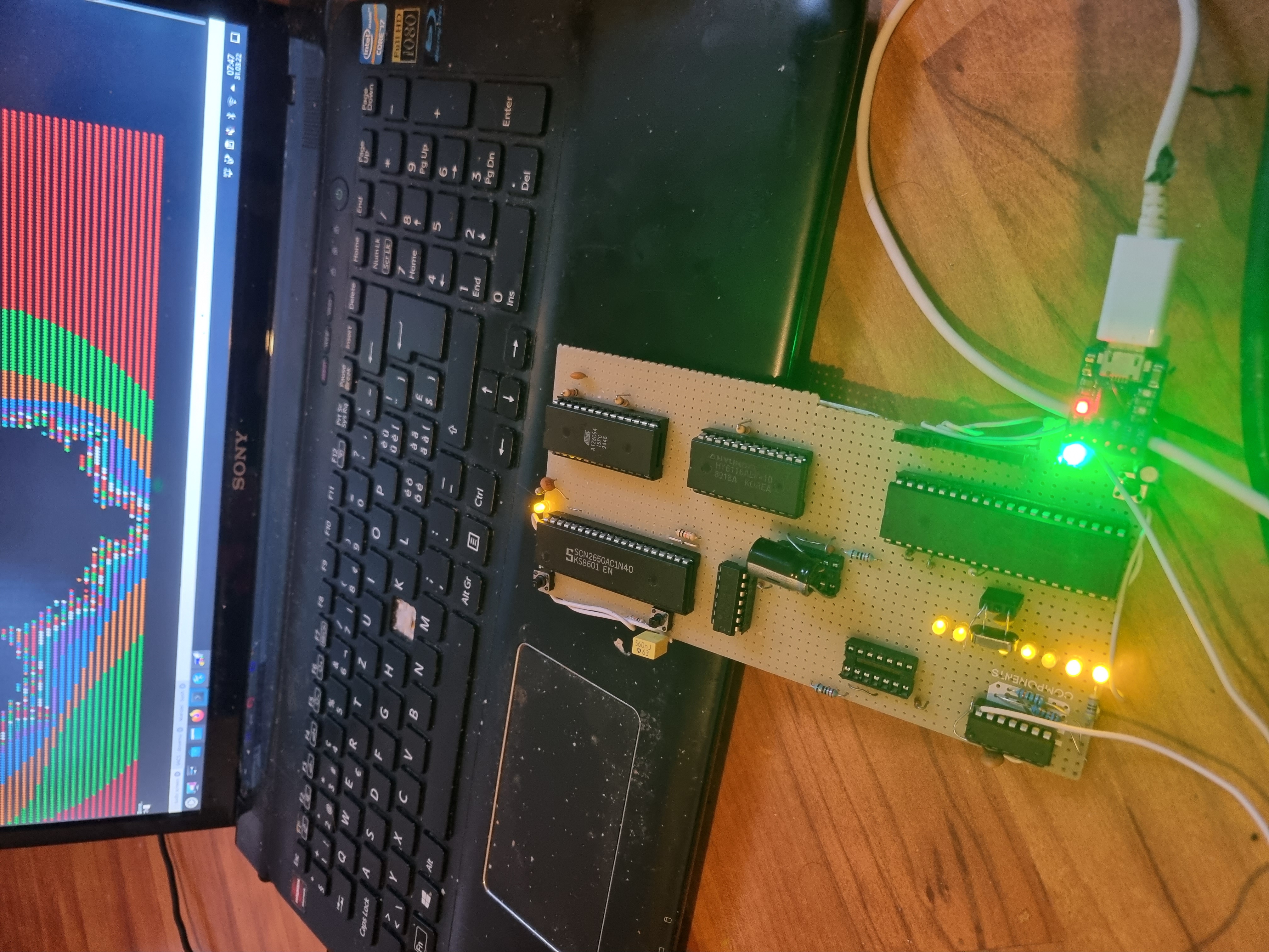
First revision of the computer board after its first successful run of the Mandelbrot program.
The first revision of my 2650 computer was based loosely on the example schematic provided in the CPU’s datasheet. It featured just the CPU, a ROM and a little bit of RAM. A AVR AtMega32 was also on board. This is something I try with all my boards, to try and get in-system ROM programming to work. The Microcontroller is hooked into the address and data bus, and some of the CPU’s control signals. Idea is that it’ll allow me to re-program the ROM without having to remove any chips.
Too bad it didn’t work, and programming the ROM required removing ALL the ICs except the ROM and AVR. I ended up keeping it though, due to a lack of any other way to get a serial port going, I had the AtMega emulate a serial adapter IC responding to one of the 2650’s I/O instructions. Unfortunately, I could only get it to be able to send. No bi-directional data transmition yet, which limited what programs I could write for the 2650.
I also originally planned to make use of the 2650’s entire 15-bit addressing range, but didn’t realize in time that the 2650 had this really weird memory access pattern as mentioned earlier. My 16K of ROM in the lower half of the address range was split into two pieces, and separated entirely from the 2K RAM above it. Ultimately, this forced me to downscale to 4K ROM, splitting the 0th 8K page between ROM and RAM.
Luckily, I prototyped the board design on a perfboard, so this was easily fixable. But its why there is unused IC sockets on the board, from when I still needed extra chips to latch the two additional address lines.
There was also a second bug in the board design related to memory access, but I’m not to blame for that one. Because its right there in the Datasheet’s sample schematic!
The erroneous schematic from the datasheet. Click to view.
Basically what’s happening here is that the write enable on those RAM ICs is gated by both R̅/W and WRP (write pulse), and their chip enable is gated by an address and OPREQ. The problem with this is that, during a write, the 2650 will put the correct signals on the address and data buses, use R̅/W to signal a write and assert OPREQ. Then, it briefly pulses WRP.
This means that, until WRP is pulsed, the RAM ICs are addressed, enabled, but still in read mode, despite the signal on R̅/W, as it is NANDed with WRP. Very briefly, the RAM ICs start outputting data onto the bus at the same time as the 2650. A signal collision occurs until WRP is pulsed.
In my case, it was significant enough for the power spike to cause a CPU halt or reset on memory writes. Much headache ensued, although I am surprised I managed to figure this one out so quick. Its quite subtle and required several looks back and forth between the timing diagrams and the schematics.
In the end, my ˝fix˝ was it to use a 1000µF capacitor accross the RAM IC’s power lines to absorb the shock of the signal collisions. This fixed worked so well infact, I kept it permanently. Even the latest board revision still works like this.
In the end, the board worked well enough that I developed most of my software for the 2650 on it, using it to learn the architecture. It wasn’t until months later, when I had some spare income, that I decided to turn the design into a proper PCB.
Revisions 2 & 3
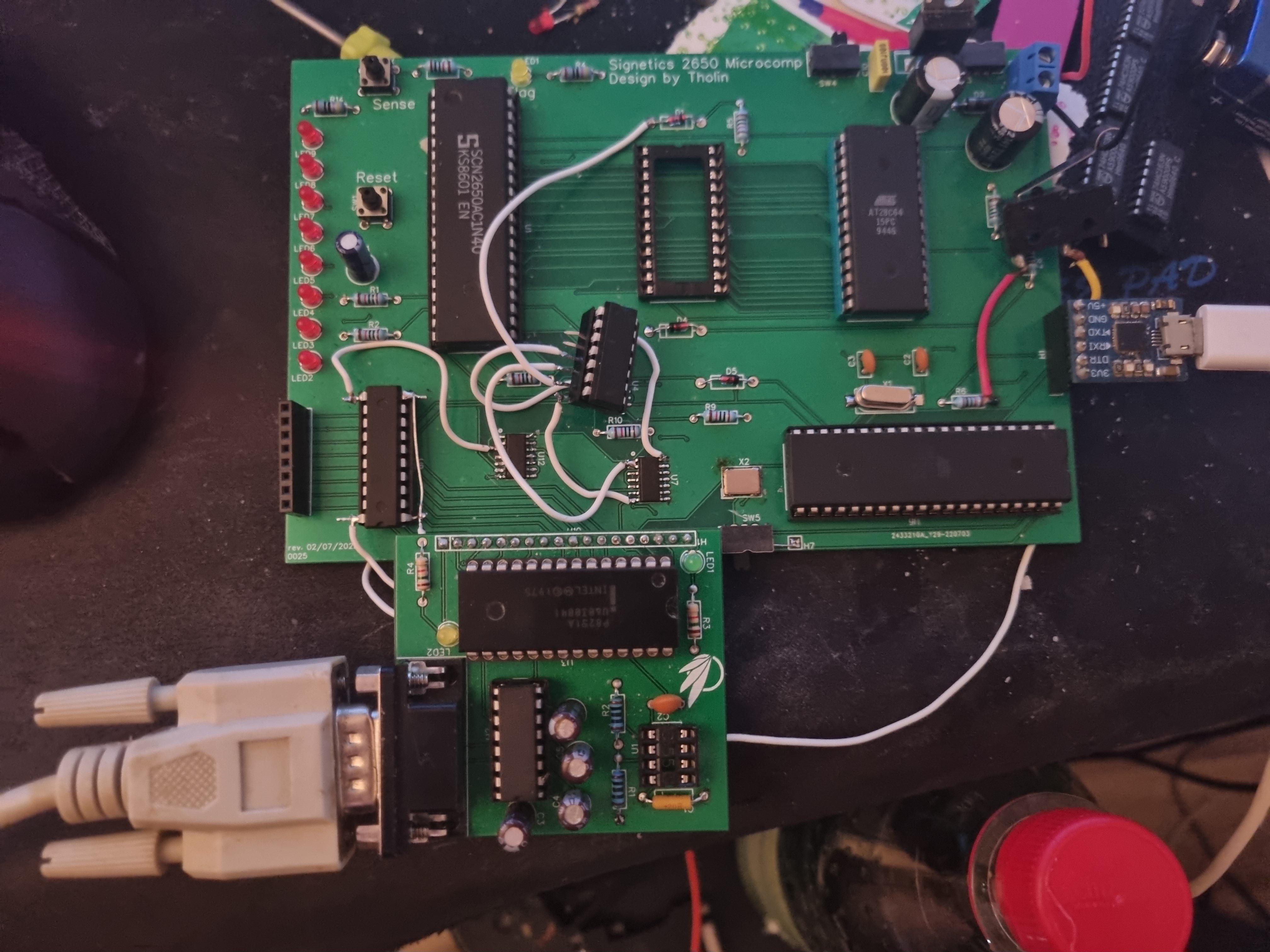
Board revision #2, in all its bodged beauty. Click to view.
Boards 2 and 3 are almost identical in design, with #3 just being a bug-fixed version of #2. And by god did board 2 need lots of bug fixes!
Its still based on the same memory setup as the original board: 4K ROM, 2K RAM, with the I/O bus used for serial. But this time, I used a module I originally developed for my 65C02 computer (which ultimately didn’t work, so I never got to test that module). It has a P8251 to give the computer a bi-directional UART, and a MAX232, to turn that into RS-232 serial.
The board also needs an additional two inputs. One for hardware reset, one for switching between command or data transfers (C/D̅ pin). I decided the best way to handle that while also increasing the functionality of the board was it to give the CPU some output ports. I used a 74-series transparent latch to give it 8 output ports, two of which are wired to the 8251’s RESET and C/D̅ inputs.
Unfortunately, the board was very broken! I made a mistake in my glue logic, on top of choosing to use SMD ICs for the 74HC00s, which ended with the uggliest bodge fix of all time, where I loosely wired up a whole other IC onto the board. In-system ROM programming was still bad, despite the addition of a switch that cut power to the whole board except the AVR and ROM. The RAM IC still needs to be removed for ROM programming to work, and this is something I did not manage to fix for revision 3 either.
I also swapped the data input and output lines on the latch IC, so I intentionally put it into its socket the wrong way around, changing the connections on just 4 of its pins to make it work that way. Only the most cursed bodge fixes are used here!
Serial was also not working. I made the mistake of not testing the serial module beforehand using a microcontroller, and did not realize that a 555 timer didn’t work for generating a precise bit clock. In the end, the microcontroller on the board was used to generate this signal also. The board was barely in a working state, and the serial bit clock coming out of the AVR was still to imprecise for receiving to work without the occasional error. I verified the board design as much as I could, and used it to build some driver subroutines for the 8251 to pass the time while waiting for fixed PCBs to come in.
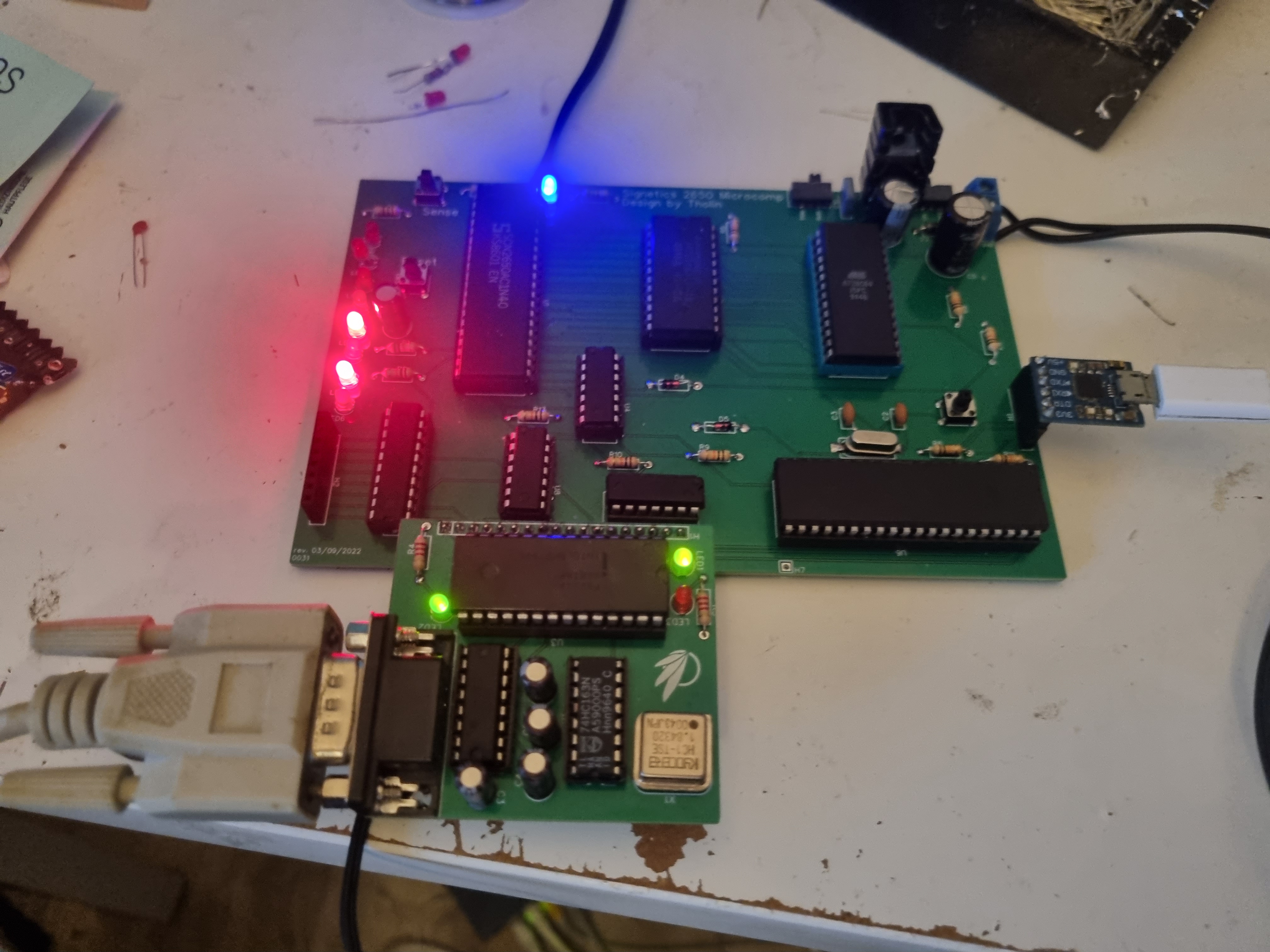
Board revision #3, finally bug free! Click to view.
The third version of the board is about as close to perfect as it’ll get. It requires no bodge fixes to work, but still needs to have the RAM IC removed for ROM programming to work. The only improvement I can think of would be to replace the ROM IC socket with a ZIF socket, and just accept that it needs to be removed from the board to be programmed.
I also used DIP ICs everywhere now, to make it easier to build, and to make any potential fixes easier.
The serial module is also perfect now, and I will definitely be re-using it for future computer builds. While experimenting with the failed module, I discovered that the 8251’s clock can be independent from the system clock, and I used this here to make the module independent from any of the clocks on the board it is plugged in to.
A 1.8432MHz oscillator is used as the base clock fed directly into the 8251, but its also divided down by 8 by a 74-series binary counter before being fed into the 8251’s RX and TX clock inputs, where it is divided by 16 again, to arrive at the final baudrate of 14.4K.
The UART is also finally bi-directional! For the first time, I could program a simple shell that lets me enter data into RAM, and execute it. I am also looking into using this UART to allow the 2650 to create some interactive programs, maybe some games. Using the output ports in combination with Sense for serial in to bitbang SPI devices in software is also something I want to try.
Toolkit
Getting a working dev toolkit going for the 2650 was difficult. The only functional assembler I found was an ancient DOS program, and of course, there was no emulator. At least, none that I could extend to emulate my exact hardware setup. Ultimately, I ended up using C# to make my own. Both are only mostly functional. Both the assembler and emulator don’t know some instructions, but this should not be a limiting factor in most cases.
I’ve open-sourced this entire project on GitHub. The repository contains documentation on the 2650, the project files for the board design, a bunch of example programs, my dev toolkit, the firmware for the AtMega32 and the ROM programmer software.
You can check it all out right
Here!