
MC14500 bit-serial computer
This is definitely one of my "I just want to see if its possible" kind of projects, though its probably the most interesting one. By the end of it, I found myself questioning what it even means to "compute" something and how far the concept of a RISC Processor can be taken to its logical extreme.
This journey begins with me discovering a quite unusual chip, thanks to the Usagi Electric YouTube channel.
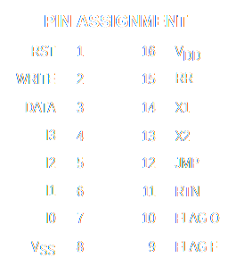
MC14500 pinout
Usagi is correct in considering this IC quite fascinating. It markets itself as a 1-bit processor, as evident by the single-wire databus in the pinout. It is capable of performing logic operations between single-bit data and a 1-bit accumulator register, called the Results Register, but the purpose of this chip is not immediately clear.
That is, until you go back to when it was released: 1977. Back then, a lot of digital control logic in industrial applications was built using TTL logic, discrete transistors or even mechanical devices. The Idea of putting a whole microcomputer or even a microcontroller, an invention that was barely 3 years old by then, into some kind of control unit was ludicrous. It was simply too expensive.
Then, along comes the MC14500. Simply wire up some input and output latches to it, maybe a few bits of RAM and you could define your control logic in software and burn it into a ROM. Instead of using, say, TTL ICs, just program the MC14500 to compute the same kind of logic operations as those ICs.
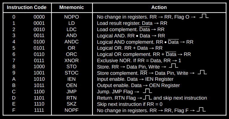
MC14500 Instruction Set
The instruction set of the MC14500 supports this use case as well. A instruction input 4-bit wide means only 16 possible opcodes, but that is more than enough for the ICs intended use case and leaves 4 bits of a standard 8-bit ROM free for use as an address to either IO or memory devices.
Looking at the opcode tables reveals mostly logic operations and some load/store types. NOPO, NOPF, JMP and RTN actually all do nothing internally. They simply pulse one of the IC’s output pins, making the naming of JMP and RTN entirely arbitrary. Really, all of these opcodes are meant for the designer to implement custom operations on their circuit board.
A basic conditional 'branch' is implemented using SKZ, which conditionally skips just the next instruction. Though the intended way to do longer 'branches' is using IEN and OEN, which set the states of internal flags with the same names. If OEN is de-activated, all store instructions cease to have any effect. The WRITE flag is no longer asserted and the data bus stays high-impedance. This de-activates execution for some time, allowing larger sections of code to be skipped. This kind of predication is very useful if you don’t have an actual jump instruction or even a program counter. That’s right, the MC14500 expected the PC itself to be implemented by the designer using TTL counter chips. This meant that most implementations of a MC14500 system would have it simply loop through the whole ROM repeatedly with no way to branch, which is where IEN and OEN would’ve come in.
Now that we’re familiar with the MC14500 and the original intentions of its designers, lets see about using it in ways they never would’ve dreamed of. But first, I need to explain the Idea behind
Bit serial computing
A normal computer processes data in parallel. This means that you may have, for instance, an adder with two 8-bit wide inputs, and one 8-bit wide output, plus maybe a carry out. Plugging two 8-bit numbers into the inputs will immediately produce the full output. A bit serial computer, in constrast, steps through the input data one bit at a time. Instead of a full 8-bit adder, it only has access to a single full adder stage. So, it starts by adding the least significant bits of both inputs to get the least significant bit of the result plus the carry into the next stage. On the next clock cycle, it takes the next pair of bits to produce the second bit of the output and so on.
The main advantage of this is, of course, reduction in complexity. This is why a lot of early computers built around TTL ICs or even discrete transistors worked like this. Though even in the modern day, bit serial RISC-V cores exist to take advantage of the area savings when put onto the die of an IC or the LUTs of an FPGA. Of course, bit serial processors are nowhere near as fast as their parallel counterparts, but that doesn’t always matter. It is often physical size that is the limiting factor.
However, all of these bit serial computers have one thing in common: they still present themselves outwardly as regular parallel processors. A regular RISC-V core and a serial RISC-V core both process the same 32-bit wide instructions and its not until you look under the hood that you can tell the difference. This means that a lot of complexity goes into microcoding and sequencing the bit serial processing from instruction data meant to invoke the appearance of a parallel processor.
I believe an even more simplistic approach is possible, using the MC14500 as a core. Not only will I get rid of complex instruction decode, but also further de-bloat the design by sticking to only the logic operations available in the MC14500 instruction set.
In Theory
There’s a couple of problems that need to be solved before the MC14500 can be used as a more general-purpose CPU. Assuming I’m indending to process 8-bit words, I need to know how to do the following:
a) Arithmetic
b) 'True' branches, none of that predication stuff
c) Connect enough RAM to be usable
d) Some kind of interface for me to interact with it (serial console at least)
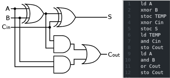
A full-adder and its equivalent in MC14500 code
Starting with arithmetic, this one feels tricky at first because all the MC14500 lets you do is compute logic operations such as AND, OR, XNOR. There is no ADD and no carry register. However, this one is solvable by literally using the MC14500 for its intended purpose: replace logic circuitry using software. The smallest unit of the logic circuit used to compute binary addition is the full adder. It is only a few gates and thus easily translated into MC14500 code. Copy-paste 7 more times and you’re got an 8-bit adder.
However, as seen in the graphic, computing this operation requires one 1-bit memory location to hold some of the adder’s state temporarily, as all of its logic gates can only be computed one at a time and the paths diverge at multiple points. Also, the carry to go into the next stage needs to be stored as well. Of course, adding some 1-bit RAM to the computer wouldn’t be difficult, but addressing a decent amount of memory, say 256 bytes, would quickly become difficult if it had to be bit-addressed. Especially if the memory address has to come out of the program ROM. I’d really like to go with a solution where only the 4 remaining bits of the ROM are used as an address, but that only gives 16 possible memory locations.
Luckily, the solution for this problem can be found by briefly moving on to the next item on the list: branches. The main problem here is that the MC14500 does not have an internal program counter and 74-series counters will instead have to be used. The MC14500 cannot simply set the value of this counter all at once with its only 1-bit wide data bus, but why even try doing that in the first place? It would be acceptable to have some kind of buffer sitting between the MC14500 data bus and the program counter. Lets call it the Destination Register, as it will buffer the branch destination before the execution of a JMP instruction triggers a load of its value into the PC. Of course, trying to map each bit in this counter into the 4-bit address space will quickly eat up all addresses, but that is when we meet the absolute savior of this whole project: the shift register!
Shift registers are very neat, allowing data to be loaded into it serialy, one bit at a time, either LSB or MSB first. A number of those loads later and you’ve got a whole word of information latched just from 1-bit transfers. This will be the Destination Register, allowing the MC14500 to (slowly) branch to any location in ROM it likes.
This is also how the RAM problem is solved! The computer can totally have a handful of 1-bit, directly addressable scratchpad RAM locations for quick access, but for accessing greater amounts of RAM a shift register can be used to buffer a larger RAM address. Infact, the RAM doesn’t even need to be bit-addressable anymore. Shift registers can also operate the other way around, latching a parallel data word and presenting it one bit at a time. Every time that bit is read, the word is shifted and the next of its bits presented.
This means shift registers can be used to buffer data going both in and out of a regular old 8-bit memory chip.
This actually solves a lot of problems at once. Using a shift register as the Memory Address Register (MAR) means arbitrary data can be used as a memory address, allowing complex addressing modes to be defined in software. Copying a byte from RAM into the MAR equals indirect addressing and performing an addition on that byte before putting it into the MAR is the same as indexed addressing.
And using these shift registers to buffer data going in and out of the RAM makes it so much easier for the MC14500 to step through bytes one bit at a time. I will call these buffer registers the Data Out Buffer (DOB) going into the RAM and the Data In A (DIA) and Data In B (DIB) latching data coming out of the RAM. Two input buffers as some operations (addition, subtraction) require two arguments.
Lastly, the computer needs some kind of interface to talk to me with. But driving a serial port is literally the one thing a 1-bit processor will be good at, so this isn’t even really a problem, I just need to get the timing right. Though I also include a clock signal next to the data line just in case.
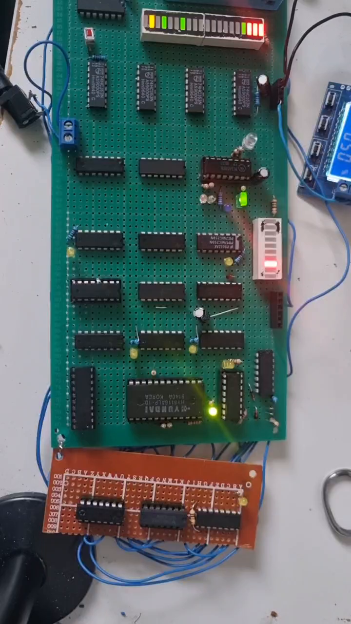
The Board!
The Hardware
For the actual hardware build, I decided to go with an 8-bit word size as 74-series shift registers of that size are available in single ICs, though that decision is entirely arbitrary. It would be just as easy to make it 16-bit or 32-bit. The exception to this is of course the Destination Register, which is 16-bit wide to match the size of the PC (I also accidentally wired it up as MSB first, while the rest of the shifters are LSB first. oops).
The 4-bit direct address space of the MC14500 is split into an 8 x 1-bit large scratchpad memory starting at address 8, and 8 addresses starting at 0 in which all the shift registers are mapped. Address 0 is made to always read a logic 1 through a pull-up resistor on the bus, to allow for immediate loads and to initially enable IEN and OEN.
The serial port is actually implemented through the scratch memory. The bits at addresses 14 and 15 are used as the serial clock and data respectively. This setup can only output data, but a full-duplex SPI-like bus could be implemented by mapping a serial input into an unused address, of which there are actually multiple (I finished under-budget, it seems).
As discussed earlier, shift registers are used to buffer data going in and out of a 8-bit RAM on the board (a 2KiB RAM of which only 256 bytes are used as the MAR is also only 8 bits wide). However, the actual read and write operations still need to be triggered on it after address and data setup are complete. For this purpose, I am using the NOPO and NOPF instructions. NOPF triggers a store of the contents of DOB into RAM at MAR, and NOPO triggers a load of data from RAM at MAR into either DIA or DIB depending on which one of them the 4-bit address provided with the instruction is pointing to.
The board generates a 2-phase clock from a single clock input. The MC14500 only takes one clock cycle per instruction, but it does this by doing things on both the rising and falling edges and the shift registers also need a discrete point in time to latch data and/or shift, leading to timing violations if this all tries to happen on the same clock. A 2-phase clock is basically required for things to run smoothly.
In the end, this design comes out to very little ICs even compared to those bit serial TTL minicomputers. Though I do end up running out of board space at one point and have to extend the perfboard a little. Still, the density of this design could probably be perfected even more by using actual PCBs (something I should’ve done instead of suffering through manually wiring
all this
).
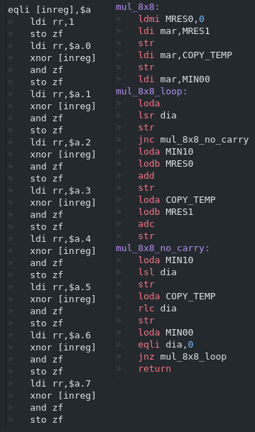
A macro definition for number comparison (left) and a code sample for multiplication (right)
The Software
This was probably the most difficult part of the whole project. Finding a way to efficiently program this computer to process 8-bit data when all I have access to is the MC14500 1-bit instructions. Of course, the use of assembler macros comes to mind. But the real complex macros would probably have macros inside them and maybe macros inside those macros. Basically, I decided to build a custom assembler with a focus on efficient macro resolution and being able to define macros in a separate file.
A lot of time was spent just writing, testing and documenting these macros. However, the effort was well worth it. Writing code for my MC14500 computer is now as easy as writing code for any 8-bit processor, as seen in the code sample. I even got subroutine calls and returns going, although the return addresses are determined during assembly, but I believe I can live with my code being non-relocatable. On something that is effectively a Harvard Architecture computer, it barely matters anyways.
I also built a simulation of the computer in Verilog. Its very detailed, using models of not just the MC14500, but all 74-series ICs used in the project. It ended up helping out a lot, allowing me to track down bugs that, in hindsight, I had no chance discovering with just the real hardware and a simple logic probe. It also, of course, allows me to test my macros and software.
The first thing I tried to code was that multiplication routine in the code sample, during which I discovered how absolutely horrible the code density of this is. Something as simple as that routine easily expands into over 1000 MC14500 instructions. However, the resulting program does successfully multiply numbers. And now that I can multiply numbers...well, if you know me, you know where this is going:
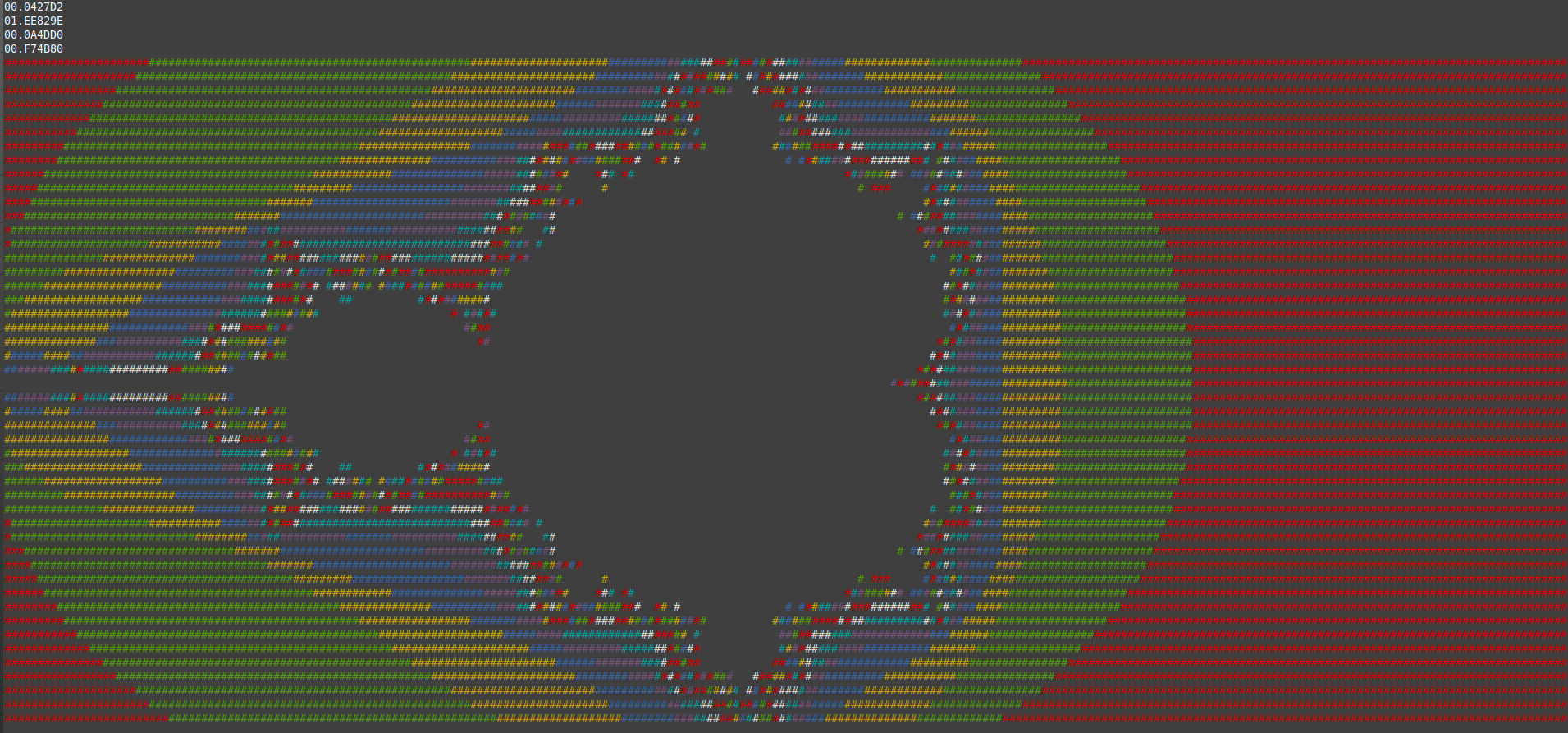
The ROM image for this is a whole 19.2KiB
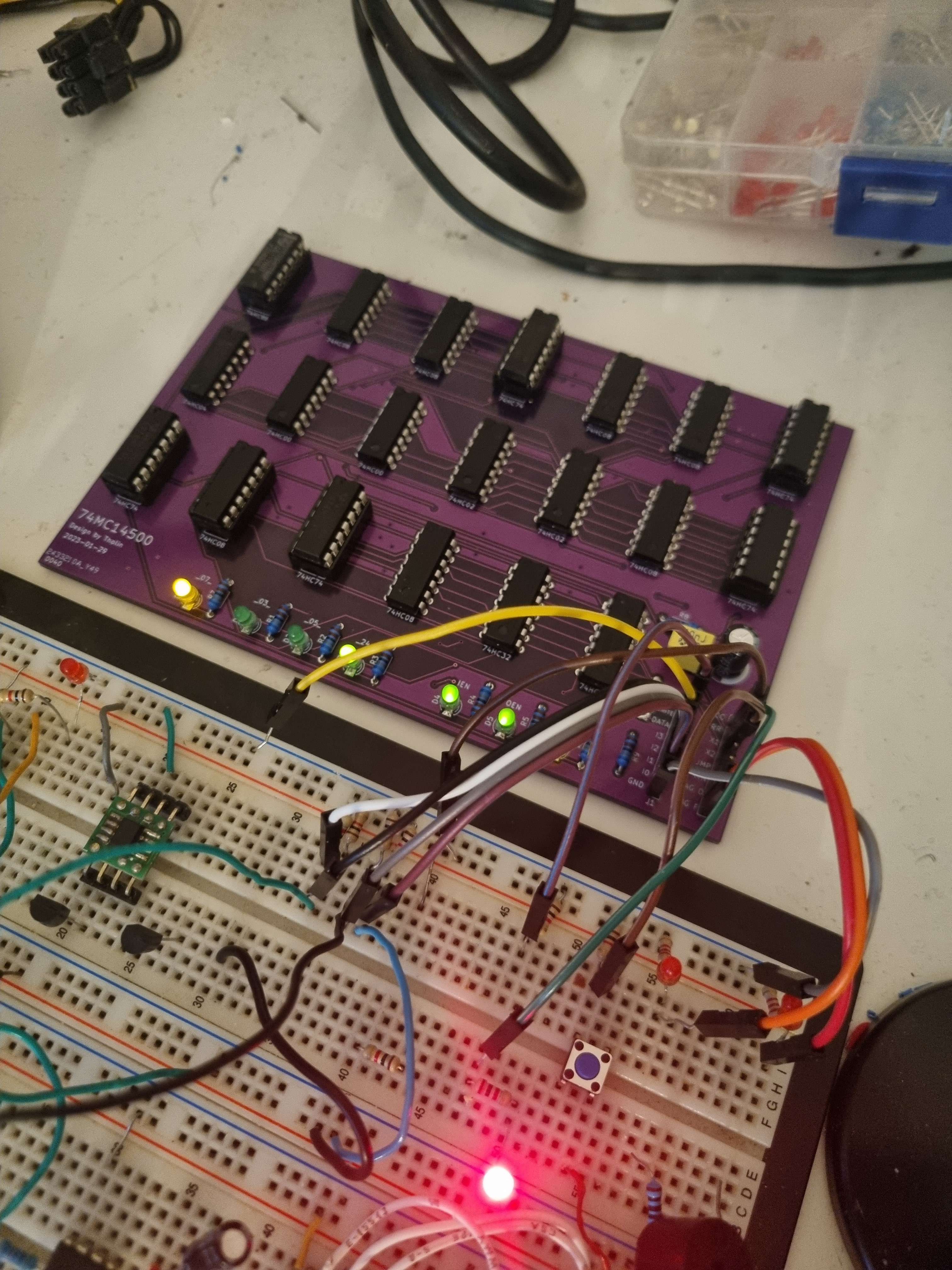
The 74-series MC14500 undergoing testing
Conclusion
As I said at the start, this project really made me question things. Even being restricted to 4 logical operations, you can still compute anything, as proven by that Mandelbrot renderer. Its quite magical watching this thing run along on my desk, doing nothing but ANDing, ORing, XNORing, complementing and shifting, but still doing complex arithmetic.
I’ve almost certainly achieved my goal of building probably the most minimal bit-serial computer to ever exist. Of course, I’ve just offset the complexity, but this time purely into software. And with how cheap ROM is these days, I have no issue with that. I do wonder if something like this would actually be useful as a super minimal on-die microcontroller core for debugging purposes in ASIC designs. If the MAR was expanded to 16-bits, the address range would be just large enough to be useful, allowing debugging interfaces, such as logic probes, to be memory-mapped.
A C-compiler for this architecture also wouldn’t be out of the question. Because every instruction is just a macro, optimal instructions for building a compiler backend could be engineered at will.
However, I don’t think I’ve hit peak minimization yet. The MC14500 is still very bloated, featuring instructions that are useless for my purposes, such as IEN (and even OEN, really) or RTN. I wanted to use the RTN flag for something, but ended up just not needing it (I also realized too late that it always skips the next instruction, which is annoying). NOPO and NOPF for triggering RAM reads/writes could also be wrapped into one instruction, with the MSB of the argument deciding between a read or write operation. Actually, JMP could be included in this as well. Some of the load/store instructions are also a bit redundant with how I use them. ANDC and ORC are also pretty useless to me. It may be possible to reduce the architecture to just 8 instructions without worsening code density at all, which is an absolute win in my book.
I did, at one point, decide to come full circle and build a MC14500 out of discrete 74-series logic, so making a custom 8-instruction processor would almost certainly be possible, but then it wouldn’t be a MC14500 computer anymore, and that was partially the point of this project anyways. So I don’t believe I will pursue any further optimizations.
Repo
If you somehow feel like checking out this absolute madness, I threw all the files related to this project into a repo here.