
i8085 SBC
This machine was supposed to be a little side-project, but quickly grew a bit out of proportion on the software side. I mainly built it because I wanted to see if I could boot a system off of SPI and I²C ROMs for faster iteration when developing software. However, it has barely any IO as a result.
Hardware
The hardware consists of an Intel 8085 at the core (80C85 also works), with a 32KiB ROM and 32KiB RAM. Initially, a 81C55 was intended to make up all of the IO. This chip combines 14 I/O ports with a timer and 256 bytes of SRAM, and makes it so that the computer can technically be run without the 32KiB RAM IC. Though in my case, I just wanted the I/O and timer in one package. However, 14 ports ended up not being enough, so a 74HC573 is memory-mapped to provide 8 additional outputs (labeled as "extra outs" in the code).
There is a slot to put my UART module into, however, I was afraid that it would not be able to keep up with the high speeds the 80C85 can run at, and so a large amount of I/O ports on the 81C55 are wasted to talk to it. This was, in hindsight, probably not required. I did, however, add a second header for this "slow bus" so another peripheral board with the same pinout could be attached. If I ever make more.
The memory map thus consists of ROM at the first 32K addresses, the 256 bytes of RAM in the 81C55 following that, followed by the 32KiB RAM IC up to the final 256 addresses, which all map to the extra outputs. There is also a memory layout that should be respected by software, where the first 256 bytes exclusively belong to the stack and library routines. It should only be accessed by user programs when accessing parameters to library routines.
All the glue logic has been reduced to a single GAL22V10 (substitutable with a ATF22V10C, which are still being made and often in-stock), and a second 74HC573 is used as the mandatory address latch responding to ALE. The GAL also makes it so that the timer expiring can regularly trigger a RST7.5 interrupt. The timer is clocked using a 555, so it can be configured for longer intervals, at the cost of lower precision, and can take up to several seconds to expire. A push button is wired up to the TRAP interrupt (it is software de-bounced), and a special breakpoint routine allows pausing program execution until the next TRAP interrupt, to help with debugging.
Of course, the main feature of the board are the headers for SPI and I²C ROM "cartridges". Both are driven in software by the I/O ports. I²C is a bit extra, of course, and requires a setup with a diode and resistor to allow the bus to be floated. The I²C cart can hold any 24Cxx series EEPROM (currently only works with 24C32 due to a bug), and the SPI cart has a 3.3V voltage regulator and 25-series flash ROM, with resistors to shift the input voltages down from 5V. This way of level shifting is technically suboptimal when it comes to the clock, but I’ve yet to run into any issues, and even if I did, it could probably be fixed by using lower resistor values in the voltage dividers to achieve faster rise and fall times.
To program the ROMs, I built a small adapter to be able to connect the carts to a USB ROM programmer, though the I²C ROM can also just be removed from its DIP socket for programming, which I definitely recommend for ease of use. However, it is entirely possible to program either ROM in-system using data received over the UART, though I have yet to write code for this, as I have no issue moving a small cart between two headers. On the PC side, either method would require using a special app to push the data to the ROM, so nothing would be different there anyways.
Software
The 32KiB EEPROM on the SBC contains both a bootloader, as well as a sizeable standard library indexed by a jump table at the beginning of ROM. When powered up, the bootloader checks first the I²C, then the SPI bus for ROM ICs. It then tries to read a null-terminated string from the beginning of the ROM, which needs to match a specific string for it to be recognized as bootable. If true, it then reads a two byte length field, and copies that many bytes from the ROM into RAM, before jumping to the beginning of that data. The running program can then access further data if needed.
To make writing programs easier, and reduce the amount of duplicate code, a large amount of useful subroutines is stored in the ROM. Programs booted in RAM can call these using a jump table in ROM. These subroutines include a Xorshift RNG, various integer multiplication and division functions, fixed-point multiplication, division and even square-root, as well as integer or fixed-point to string conversion. Subroutines to access further serial ROM contents also exist.
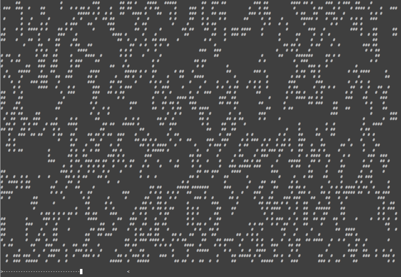
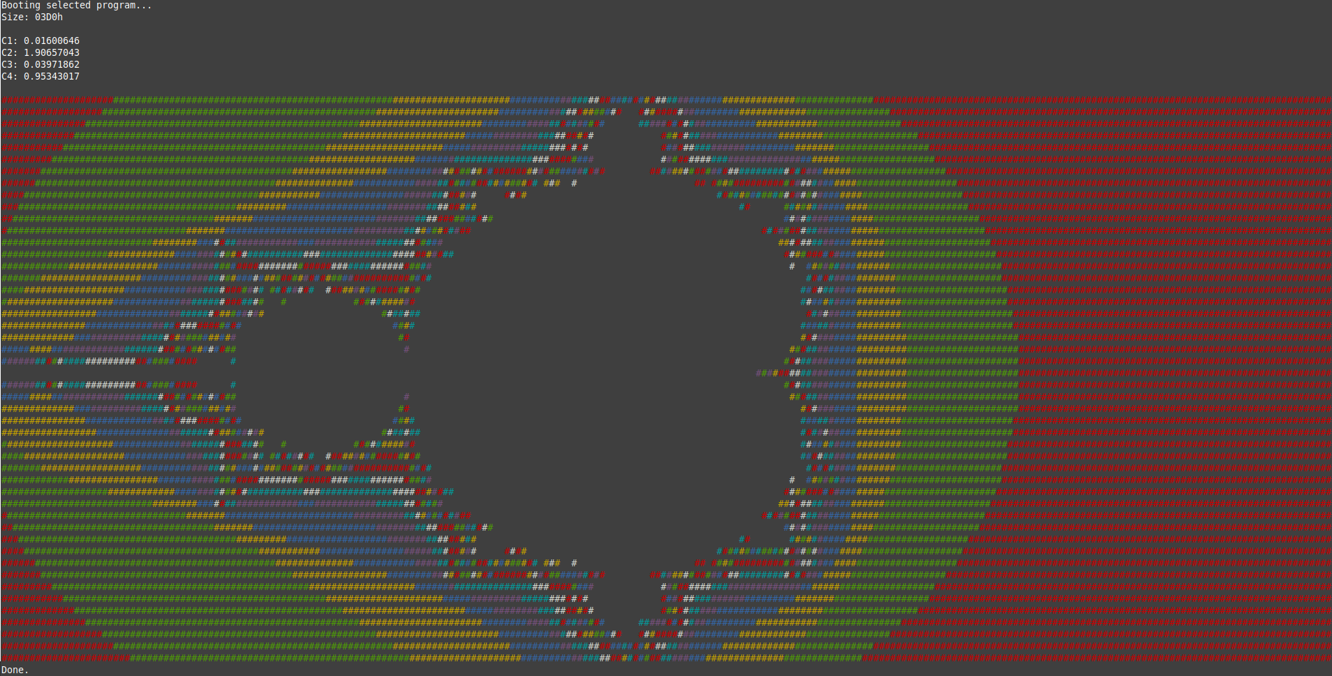
One of the pieces of software I wrote, simply called "Menu", can combine multiple programs into a single SPI ROM image. When booted, it presents a selection of programs stored on it. Selecting one causes it to be run. All of my demos (Mandelbrot, Game of Life, test for airthmatic subroutines) can be stored in a single image with it.
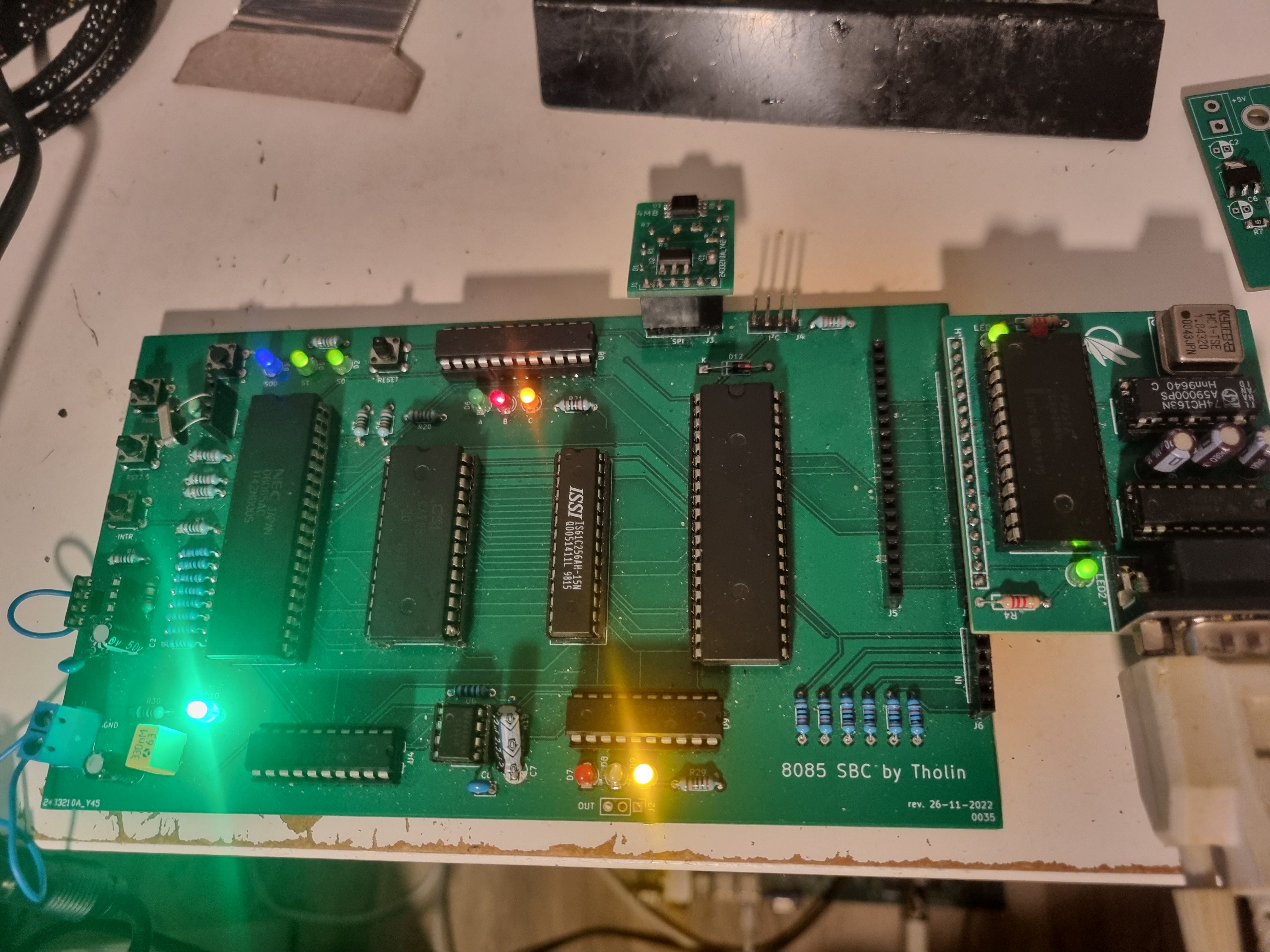
Pictures
These are a few pictures of the board, and the outputs of the demos. As with my 6507 board, this is the first revision of the board which required bodge fixes. The version of the design files on GitHub has said fixes applied to it, and will work with no changes.
Source files
As with all my computers, the source files for this project are public! This includes schematics, PCB layouts and software I wrote for it.
View on GitHub