Intel 386 con-badge
Every year for EuroFurence, I build myself a new con badge that will be seen just that year. These have been getting more and more complex each time, starting with the 1802 badge and continuing with the one using my GFMPW-0 custom silicon. However, my GFMPW-1 custom silicon was due to arrive too late for me to have a reasonable amount of time to build a badge around, so I needed to pivot to a backup plan. Luckily, I had been pondering about this since the year before: using a Intel i386 CPU to power the badge.
The i386 was Intel’s first 32-bit x86 CPU, and is still highly regarded by the retrocomputing community. It was the CPU that powered many early DOS machines (and games released for them). As such, even in 2024, it is still instantly recognizable to many (it helps that the chip has its name quite prominently written on it).
This made it probably even more of a show-off for a badge than custom silicon, so I decided to just go ahead with this idea.
Hardware selection
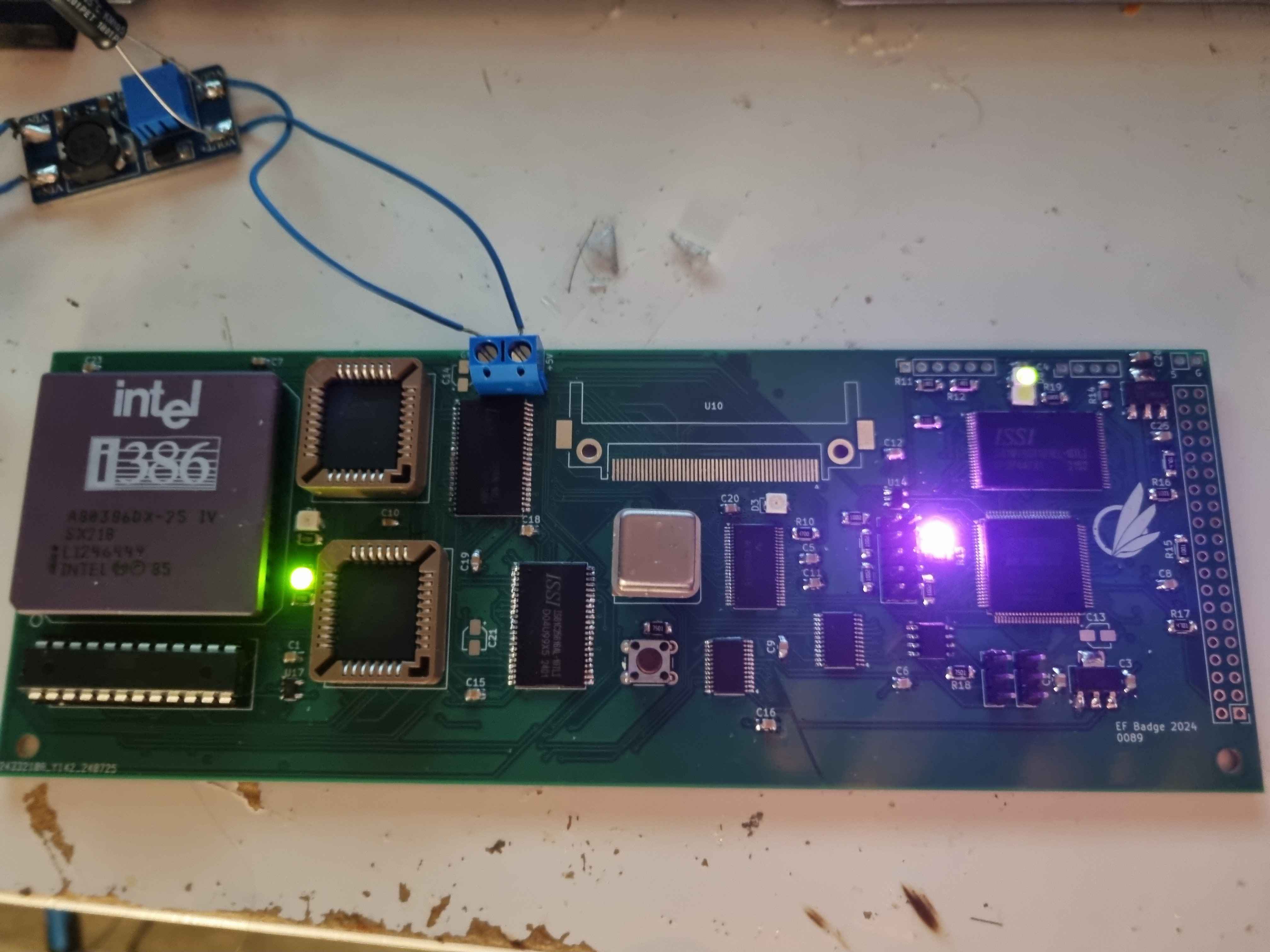
Building a basic computer system consisting of any CPU plus memory is pretty easy, even in the i386’s case. Despite all of the complexities of this CISC CPU, the actual memory bus is a simple address/data bus combination with very few bus states, making it easy to comprehend. A GAL is enough to fit all the control line generation in a compact way, just as you may see on a 8-bit homebrew computer. I settled on 1MiB of RAM, as this was simply the most I could get in just two ICs at 5V logic levels, and 256KiB of ROM to boot from.
No, the real difficulty is in getting graphical output in a compact way. With the amount of CPU power I had available now, it would’ve been sad to use anything less than a full-color LCD with decent resolution. A 800 by 480 panel and driver chip combo, with 24-bit color was chosen from AliExpress, though I would only later find out that the datasheet containing its dimensions was incorrect.
For driving such a large display, there was really no way around using a CPLD and separate VRAM again, which still required level shifters to interface with the 5V CPU. The LCD driver IC that came with the panel does have SRAM on it to store a full frame, but I wanted double-buffering, which is why a 2MiB SRAM IC is required to store a second frame.
Note that this means the buffers aren’t swapped. The CPLD instead does nothing with the display until it is told to copy its memory contents to the display buffer.
The CPU can’t directly address the VRAM, just as in my previous badge, but can ask the CPLD to write pixels for it, which maintains a auto-incremented access pointer for fast sequential writes, which covers 90% of use cases. Though the pointer can also be arbitrarily moved.
However, another problem arises here. As is already evident by the VRAM being 2MiB in size (each frame is actually 1.125MiB), a SPI flash will not cut it for persistent storage. More space will be needed to store image data. I thought that, since I have access to a wide memory bus for once, wiring a CompactFlash card directly to it would be possible. Additional wait states would need to be generated by the GAL to stretch accesses to it to ensure that timings on the card were met (same for the ROM, actually), but nothing that was impossible to pull off.
A custom PCB was also of course prepared, but with great difficulty! I don’t think I ever had to fit something this complex into just four layers. Especially around the memories and underneath the CPU, things get insanely dense. Infact, I tried to use an auto-router at first, but it failed entirely. But I was able to pull through and route it myself.
This board also features multiple clock domains! The i386 I got is rated for 25MHz, but timings only worked out for 20MHz. The i386 internally divides the clock by two (to generate a two-phase clock), so the crystal oscillator clock source is at 40MHz, which is what the GAL is clocked from. For the CPLD, though, I employed a PLL clock multiplier to boost the clock to 80MHz (mostly because the multiplier has a side effect of level-shifting the clock to 3.3V cleanly).
For power, two 18650s was used (as usual): one for the system, one for the display.
Software Architecture
Bootloader
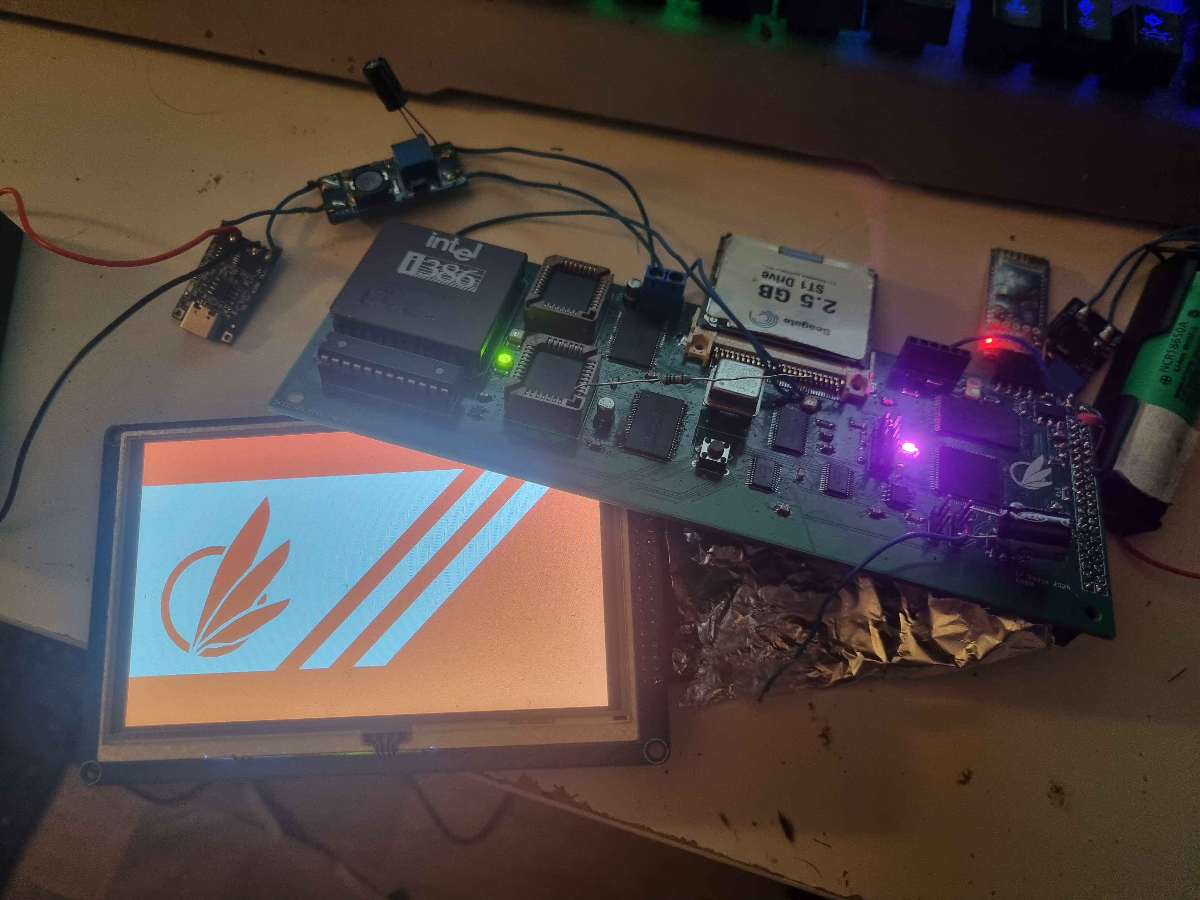
Displaying the boot logo. Bootup takes a few seconds due to the memory test.
As mentioned, the i386 is quite the complex CPU, mostly because it includes a full memory management unit. This makes booting the system difficult and requires multiple stages of bootloading. To make it harder, the CPU resets into a backwards compatibility mode where it will primarily execute 16-bit 8086 code. Contrary to what you might’ve been told, however, it can still execute 32-bit instructions in this mode through a special prefix, but that’s no way to live, so the bootloader has to transition out of that mode ASAP.
This requires setting up a Global Descriptor Table (GDT, not to be confused with the Local Descriptor Table, which I will not use here), the first level of memory-mapping the CPU has, which maps entire, continuous regions of memory (segments). This is a level below the paging unit, which maps 4KiB pages, but will not be used in this project as it would have no advantages. Instead, the bootloader will only define segments, which translate virtual addresses to physical addresses through a simple bounds check and offset.
ROM is mapped into the upper 2GiB of address space (starting address 0x80000000) and the CPU starts executing at the very top of its address space, and I reserved 512 bytes for this at the end of the ROM. I quickly found out the CPU, in this mode, cannot address the full 4GiB with the lgdt instruction, which tells it where the GDT is located, so it must be copied from ROM to RAM first. This GDT is very simple. It maps the entire ROM as read-execute and the entire RAM as read-write, with no further granularity. A stack segment is also defined, but for now, this is just a copy of the RAM segment. Now, the CPU can long-branch to the start of the ROM segment at address 0x80000000, the actual beginning of ROM, which also transitions it to a 32-bit mode.
In this second stage, can it finally bring up its peripherals: the CompactFlash disc and display, on which is shows a boot logo that could fit in the ROM. But before that, there is another thing that needs defining, which is the Interrupt Descriptor Table (IDT). It has the same format as the GDT, but defines how to handle interrupts, traps and exceptions. For context, there are many special datastructures that can be created in both the GDT and IDT, such as Call Gates. This is all in the name of operating system support. For instance, Call Gates simplify context switches by automating backing up the full CPU state. But again, I have no need for these, as I will not be running a proper OS with processes that require memory management. My IDT is filled with entries that contain simple pointers to the Interrupt, Trap and Exception handlers which it maps, instead of gates.
There are actually a couple of interrupts and exceptions that can technically happen to me at this point, such as divide-by-zero or the headache-inducing General Protection Exception, which indicates an out-of-bounds memory accesses was attempted on a segment (I got very familiar with this one). The bootloader maps these all to a handler that prints an error message and halts the system, as the whole boot process should always be the same and not be capable of causing massive problems. But from now on, if I describe actually using an interrupt, assume I have modified its corresponding entry in the IDT to point to a different handler.
The actual boot process is simple. Display the boot logo, test all of RAM, make sure the CF Card is present and okay, then start copying data from the CF Card to RAM. See, all the ROM ICs I could find were 8-bit, so without using four of them, I could only get a 16-bit ROM going. The i386 has a special 16-bit bus mode just for this purpose, but it means a drop in performance, so I really don’t want to be executing from ROM at all, actually. Reprogramming the ROMs is a pain as well (I have long surpassed the 20 guranteed reinsertions specified by the sockets’ datasheet), so better to load code from an easier to use medium (the CF card) into RAM, and run from there.
This process is mostly straight-forward. Data is copied from the first sector past the MBR straight to RAM, with the first block containing a short header to verify the data integrity. A new GDT must be constructed, however. This one is more granular. First segment is the GDT Container. As mentioned before, the GDT and IDT are stored in RAM, so I am guarding those datastructures by putting them in their own segment covering the first 4KiB of RAM. Then come the code and data sections. The former is mapped read-execute, and the latter read-write. The boot header indicates how large the code segment needs to be, with data covering the rest. The data segment is duplicated to provide the stack segment, as before. The ROM remains mapped as read-execute. But it will not be used anymore. A "dynamic code" segment is also allocated, taking some space from the data segment and overlapping with it, effectively creating a read-write-execute region. Intended to be used as a way to load more code on the fly from files on the CF Card, this went unused in the end.
The final action is a long-branch to the new code segment, completing the boot process.
Drivers
That was....a lot, and that was all just to boot the system. This basically sums up the "deal" with x86: good god, is it a lot of boilerplate and setting up the memory mapping. But now that the CPU can run the code the badge actually needs to function, lets talk drivers.
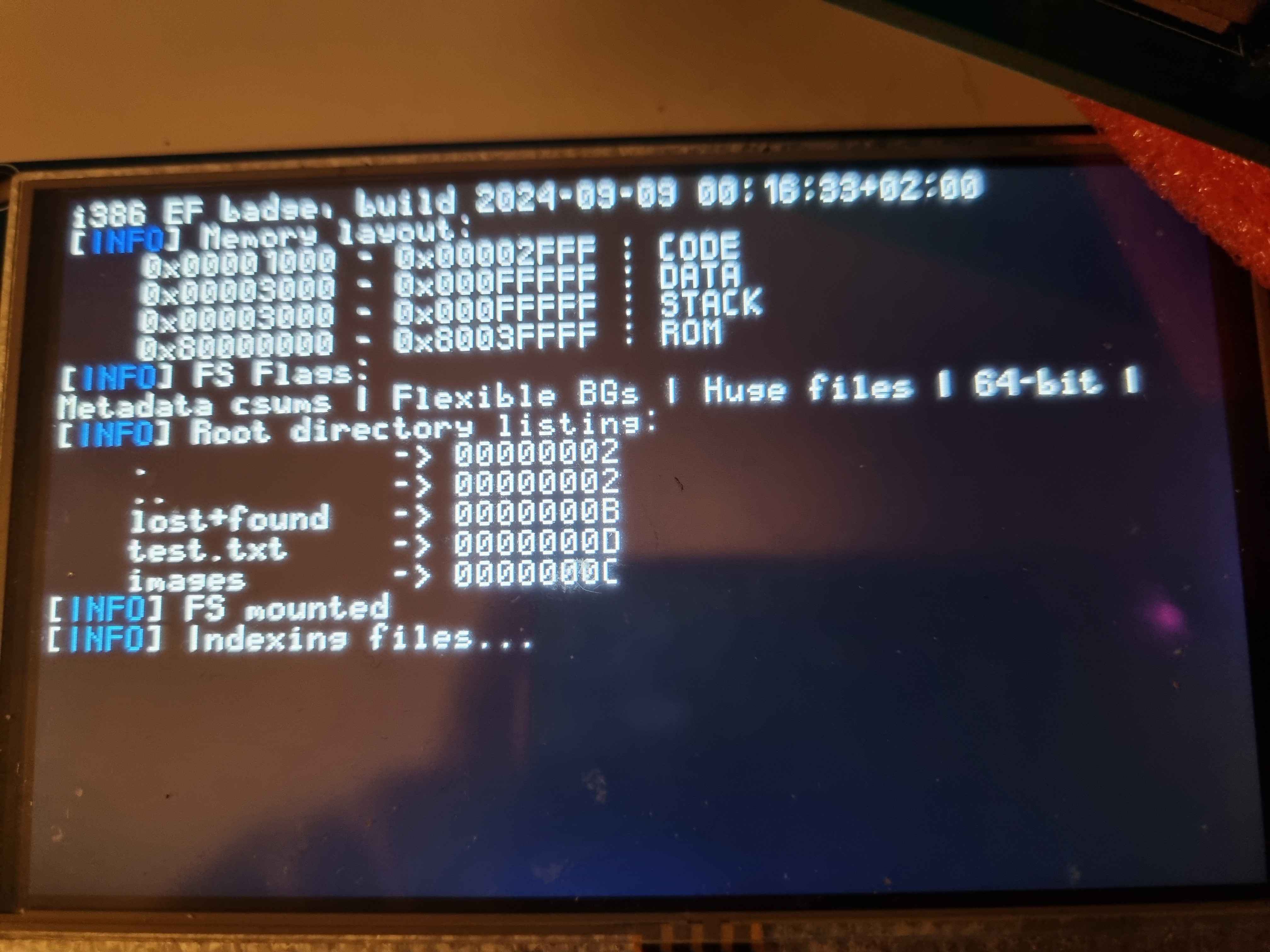
Graphics do not generate themselves and data does not organize itself. In other ways, the badge is in need of graphics routines and a filesystem. The former is not too difficult. Infact, I can mostly recycle code from my last badge for drawing simple shapes, lines and text. I wanted a way to display a more verbose boot log at this point, so a "console mode" was implemented, which supplies subroutines for printing text in a regular manner. This would help a lot with early debugging. However, images are also important. The whole reason I got a good panel for this was to be able to show photos clearly. Of course, storing images in a raw, uncompressed format would take up just over 1MiB per file on the CF Card. Its a 2GiB card, so it would’ve been fine, but I decided to implement some basic compression. I experimented briefly with running-length encoding, but instead stumbled across QOI, and decided to implement it, since it looked fun.
The end result is not exactly fast, taking 6 seconds to decode a full 800 by 480 image, as opposed to an almost instant read for a raw image, but I realized this could be a feature instead of a bug when displaying slideshows. It provided a good delay between images. Infact, the final CF Card image contained a roughly even mix of raw and QOI-encoded images.
But none of that matters if I have no place to organize those images. FAT32 is a pretty popular filesystem for embedded systems. Infact, you may have already had many encounters with the FAT32 implementation of the Arduino framework, on any number of platforms.
Naturally, I chose ext4 as my filesystem.
Okay, well, I already had C code done for reading ext4 partitions from another project, so this was a lot easier a task than it might seem. That code is quite feature-rich at this point, even implementing optional features like following symlinks and verifying metadata checksums. But for an x86 assembly port, I’d implement the pure minimum of reading files and directories and the most simple file path parser. I won’t even need to implement a seek function, forcing all files to be read sequentially.
It sounds difficult at first, but ext4 isn’t actually a very difficult filesystem. It splits a partition into filesystem blocks as in FAT32, but also groups them together in block groups. The actual file descriptors are called "inodes", containing file metadata as well as the beginning of the extent tree.
FAT32 uses linked lists to allocate blocks, which is easy enough to parse. ext4 uses extents. Each extent maps a range of blocks, going "The blocks starting at address x in the file map to address y on the disk, and this allocation is n blocks long". As these mappings take up bytes on the disk themselves, blocks may need to be allocated to hold them, which is why they are organized in a tree. Leaf nodes are the actual extent structs and interior nodes point to a specific block that will contain its children. Due to how the spec is defined, the extents are always ordered in ascending order depth-first in the tree. And a depth-first search is very easy to implement, even in assembly. And everything else up to this point is just parsing static data structures, just like in FAT32, so it really isn’t that bad.
There is no special datastructure in the filesystem itself for directories. Instead, they’re like regular binary files on the disk, with the file contents being the directory entries. This probably reduced the required amount of code by a ton, which is good. Directory entries are stored in a simple flat array in the file (ext4 does specify a format using ordering of entries by partial hashes in a tree to make it faster to find files, but I have never observed this be used in practice, even in large directories on a Linux system).
Timekeeping is the last thing I may want to do, but is easy enough. The non-maskable interrupt is wired to the CPLD for just this reason, and one is generated regularly every second or if a character is received on the debug-UART.
Anyways, that’s all the software drivers required for the system. This is what makes programming in assembly feel rewarding. You can feel yourself climb the layers of abstraction in a sensible manner. I started struggling with things like block access to the disk drive, followed by data structure parsing and other low-level algorithms, but now have a series of top-level functions that are easy to call, yet provide powerful access to graphics routines, filesystem functions and file format decoding.
The cool stuff
Finally, the good stuff. What I came here for. Would you believe me most of this was just for showing some slideshows? Well, I mean, its still supposed to be a con badge. Its supposed to show information about myself and my projects before diving into one or two demos. I believe I’ll spare the details of how I composed the slides, as, yes, it took a bit, but was mostly tedious and boring work. The end result looks good, though. Much greater visual quality than a dot-matrix display, and the panel has a good enough backlight, even during daytime. If only I had realized it comes in two sizes. I engineered the PCB around the large version before buying the small version. Now its too small, which makes it less visible and it has to hang from strings from the PCB. But no time to fix that now.
Really, the lack of time is why there is so few demos. How little time was left when I finished this? I was programming the demo I am about to explain while at the con. Yeah. See the section after this one for an explanation as to why things got so close. Funnily enough, this isn’t different from last year, where the same thing happened due to the fact I was working with a buggy CPU, which increased all my development time drastically.
Anyways, there is one demo on here worth talking about. The rest are copies of stuff from last year, such as showing the uptime and drawing sine/cosine lines (which are way less impressive on a 386, tbh). Last year, I ended the series of demos on my badge with a crude 3D render. I wanted to do that again, but in much greater quality this time.
The idea was the same, though I did start over on the code, which is software rasterization. Raytracing may actually be implemented in less code in a pinch, but I am familiar with both algorithms, so I decided to go with the more performant option, even thought it meant still making updates on it way into the last day of the event. I would once again like to thank the Scratchapixel guide on software rasterization for the detailed reference.
Rasterization involves doing all the math required to project points in a 3D space in a way to make it look as if they were being observed from a particular perspective. This is the key to making things appear 3D by having objects become smaller as they move farther away, or for different faces of them to become visible as they change position in space.
So, I called upon my old friend fixed-point numbers. I do understand floating-point numbers, but I would’ve had to implement them in software as I am lacking the i387 FPU. That would’ve meant a performance hit I did not wish for.
After projection, each triangle on-screen is considered and must now be filled in. There is again handy math that does double-duty for telling if a point is inside a triangle as well as providing interpolation values. Special properties such as normal vectors, vertex colors, depth, texture coordinates and custom properties are only defined for the corners of a triangle. So to get accurate values of these for every point inside the triangle, the three corner values must be interpolated between. This is really the key to making pixel shaders work, as it provides all the information required to uniquely color each pixel.
And that was another goal this time. The last year’s 3D renderer would do a basic interpolation of only the vertex normals, and color pixels based on the normal values to get a colorful image. Not like any detail could’ve been made out on that dot-matrix display. But now, I had enough resolution to do some proper rendering.
Beyond that, interpolation is actually required if you have a depth buffer, as the depth of each pixel in a triangle must be considered, compared and discarded if there is something already in front of it. My system still only has 1MiB of system RAM, however, which is still not enough to fit a full frame of pixels. The renderer has to write each pixel rendered to the VRAM as it is completed, which is fine, but this means a full depth buffer will not fit either. The buffer is compressed to a range 0 - 1 for each value, so only two bytes per entry instead of three for a color, but still too large. So, resolution of the render is halved to 400 by 240. I could’ve used space on the CF Card to store this buffer, but this would’ve meant more performance losses and I was running out of time as-is.
All of this is still happening in assembly too. I know the gcc can easily be configured to generate code for an i386, but that is simply not how I roll. Especially for a project that is meant to impress.
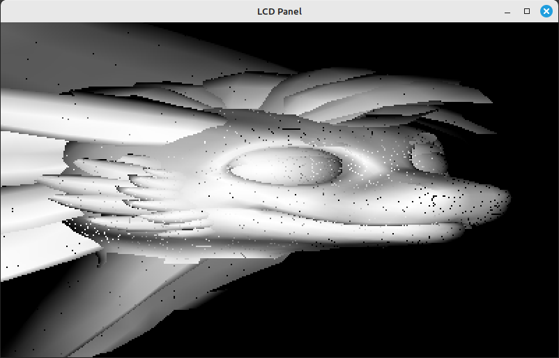
So, reduced render resolution it is, but now with proper shading, hopefully. I immediately turned to the lambertian diffuse, the easier way to estimate the amount of light reaching a point from a light source. It doesn’t take care of shadows, however, and due to the memory limitations, I couldn’t really experiment with that. Shadow casting or deferred rendering would’ve both required multiple framebuffers.
Still, it looks decent from a distance. Despite the multitude of incorrectly rendered points, that look a bit like dead pixels in the image. Yeah, I believe fixed-point of the format I used, 16.16, was not precise enough for this purpose. 8.24 might’ve fared better. Or biting the bullet and using floats.
Alas, it become too late for me to fix this, or continue on to texturing the model. Still, I walked around for about a day with the working 3D renderer. It only takes a few seconds to render my avali, with the mesh data streamed in from the CF card, so it still appears impressive.
Major issues
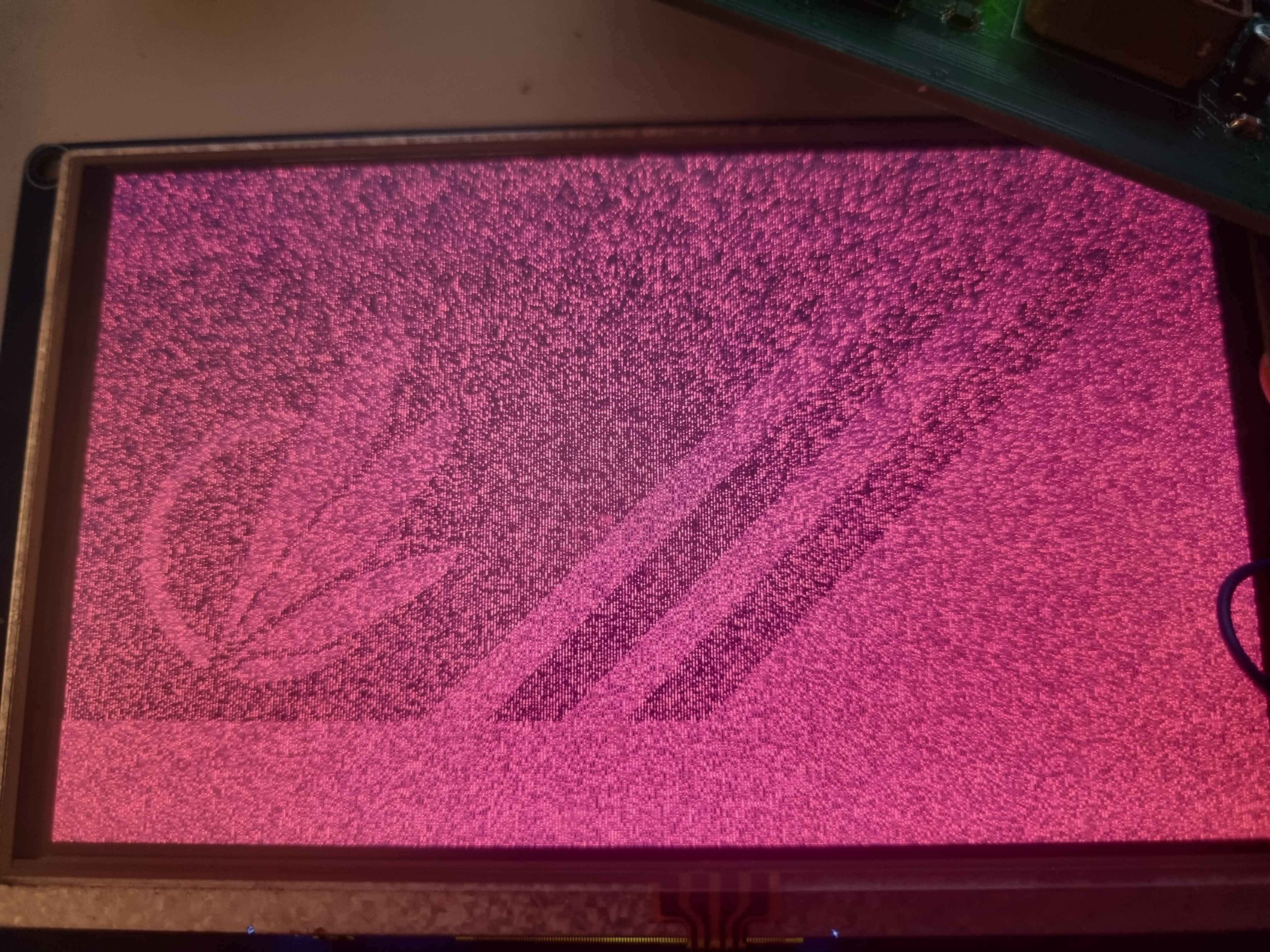
Despite how my descriptions so far may make it look, this project was cursed by major issues all the way through. After all, I did not intend to still be working on it while at the con, and even abandoned the idea of using GFMPW-1 custom silicon to start extra early with working on this. I was held up at many points, and possibly spent more time at home debugging and fixing things, than actually writing code. This truly was a project from hell!
The first hurdle was the the very, very first time I swap the ROMs from the badge back into the programmer, I bend a pin in a socket and spend three days poking at the board with logic probes and my scope to figure this out. If you see something being stuck or hot-glued into the bottom ROM socket in any photos here: that’s why.
But the main plague of this project has a rather simple name, and its EMI! It started simply, with the LCD panel seemingly only displaying heavily corrupted images. Any pixels sent to it would have a large chance of coming out with the wrong color. I could see the outline of the boot logo, but the colors were all wrong and noisy. I was aware of the problem of EMI in PATA ribbon band connectors, so this was actually not too much of a surprise to me. I tried a number of things to make it behave, even going as far as weaving tinfoil between the stands of the ribbon and grounding it, which didn’t work. That should’ve been a bad omen to me that the EMI was actually happening on the PCB traces on either side of the cable, but I was too focused to notice. The real fix was realizing that I could reduce the with of the display interface from 16-bits to 12-bits. This meant making the most-significant 4 bits of the 16-bit VRAM IC go unused, but it still had enough addresses to fit a whole frame like that. Those four lines now being permanently grounded provided additional stability, and this particular EMI problem went away entirely. Still, another long time of debugging.
There were a few minor issues on the board that had to be fixed using bodge wires, such as the control lines to the CF Card being incorrectly used. Those were the kind of thing I had allocated a margin in my schedule for. But not what came next.
The system would be extremely unstable. It would not make it through a full boot except very rarely, often running into problems mounting the filesystem or running grapics routines. But more often, it would crash with random exceptions, sometimes even in the bootloader. Just debugging the problems was difficult as the debug code would also glitch out or reveal more weird behavior. Further testing showed no problem with the memories.
In the end, I had to concede that I was dealing with severe EMI corrupting data bus contents, but just finding this out took weeks. So long, infact, that at some point I had to continue writing the software for the badge, even though I had no idea if I could get its hardware to work at all. I had set up an emulator of the system that helped me rapidly iterate on my software design, so this was possible.
I really tried a lot of things. The non-maskable interrupt line would randomly trigger due to induced voltage spikes, but a small capacitor to ground at the CPU end of it fixed the problem, and I tried to employ this strategy. Re-programming the GAL to shift some timings around provided a little relief, but not enough. I randomly soldered bodge wires between distant power pins on the PCB, with no change.
My random experimentations eventually lead me to discover that lowering the input voltage to the board from 5.1V to 4.5V would fix the EMI enough to stop the system from crashing outright. This was no surprise, as memory accesses rarely corrupted outright, with mainly IO transfers being affected. This continued to be the case, but would manifest itself rarely as single incorrect pixel values, or images occasionally becoming corrupted (especially QOI-compressed ones). But it was rare enough for me to go ahead, even though the lower voltage made me uncomfortable as it was right at the bottom of what the CPU and memories would allow, according to their datasheets.
I guess the dense routing was a bad idea after all, especially on a four layer PCB where the ground planes were entirely cut off by the density of traces around the memories.
However, all this problem fixing had lead to me massively overshooting my deadlines, leading to the described scenario of not being 100% ready once time for the con came around. And once I did arrive and powered up the badge for the first time, it was massively misbehaving again. Two crashes within two minutes (though I had since programmed the badge to recover from crashes by restarting the software).
I sat down and decided to just replace the two 18650s with freshly charged ones.
And then something magical happened. It fixed itself. The EMI problems vanished in an instant. No more crashes or even corrupted images. Just working perfectly. It was like a miracle. The EE gods were finally seeing the situation I was in, and granted me respite through divine intervention. Granted, it only stayed this way for some time, and I quickly figured out it was start acting up as soon as the voltage from either cell began dropping, even if it still had enough charge to keep going for another 15 - 30 minutes.
So, I assume the boost converters I was using with those cells introduced additional noise once they had to start working harder, despite the heap of decoupling capacitors I bodged on. Batteries of cells and linear voltage regulators probably would’ve been the way to go.
But battery life was a problem. This thing chews through 18650s faster than I can recharge them. So even though I showed up with a bag full of over 20 cells, I quickly had to start rationing them or get a little more time out of them by accepting half an hour of glitchyness towards the end. I need a better way of powering my badges, as they’re certainly not becoming any less ambitious. Either a way to charge all my 18650s at once, or a different power source entirely.
But if anything, the fact I managed to get the badge into a working state, ready to show of, probably proves my resilience and persistence. I can see a version of me that gave up long ago, and I still took last year’s badge with me to the con as a backup.
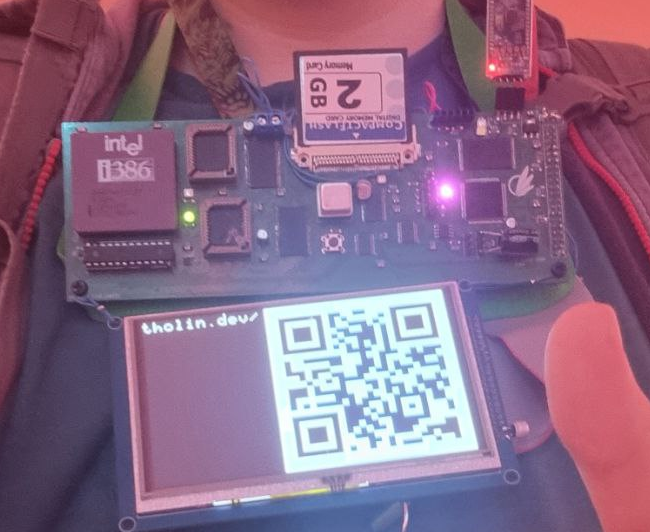
The badge in use. Note the module at the top-right, providing a UART over bluetooth, for in-the-field debugging using just my smartphone.
Repository
I’ve created a single repository to hold the source files for all of my con badges. This one can be found here.
