
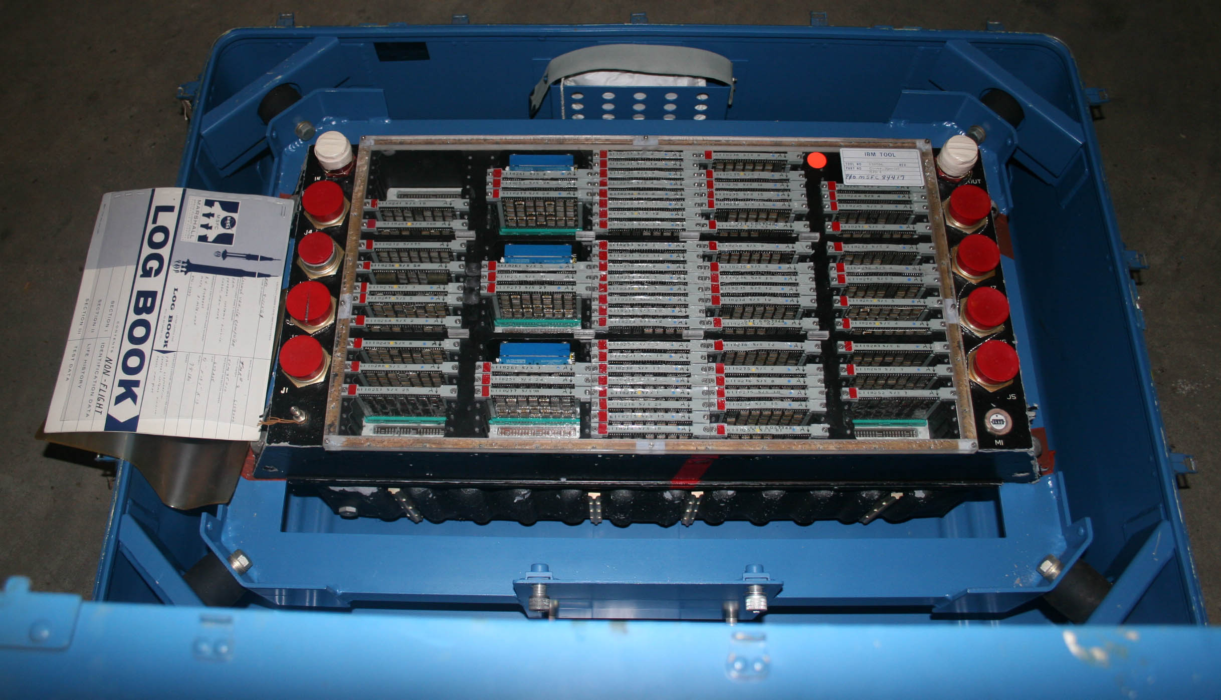
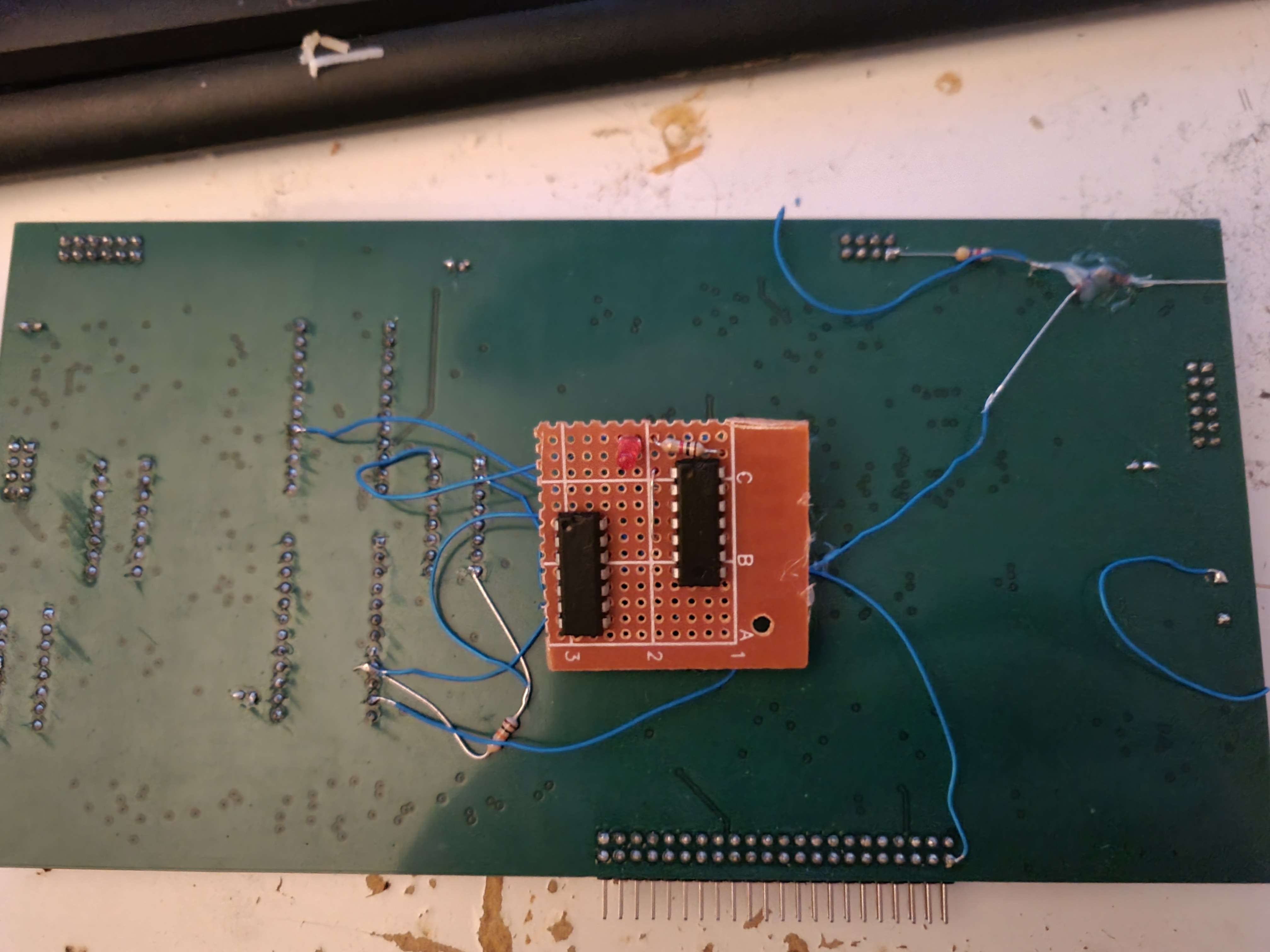
Launch Vehicle Digital Computer replica
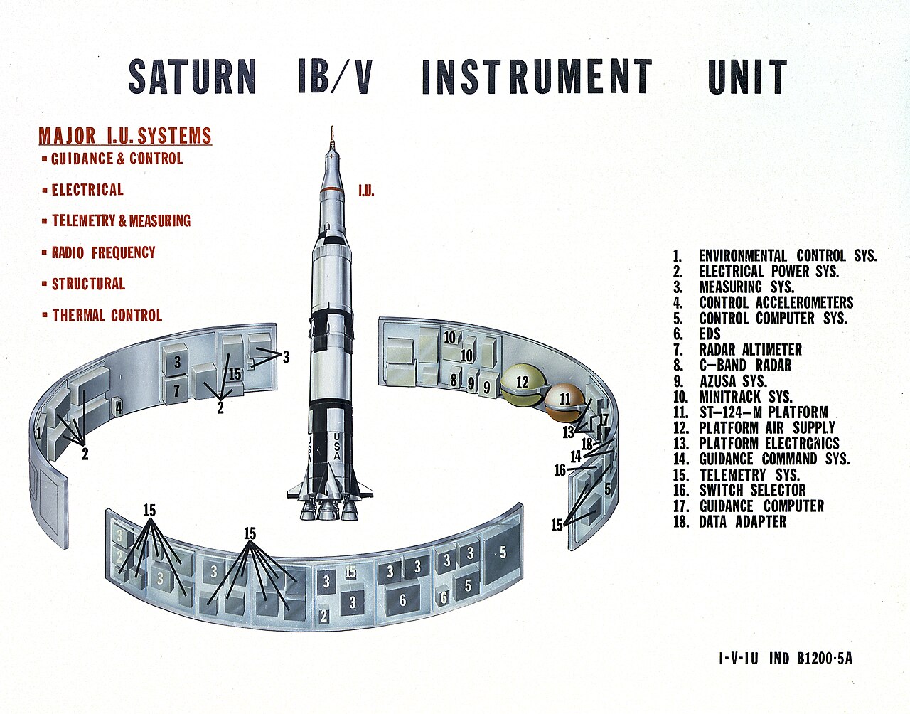
The instrument ring of the Saturn V - The Number 17 marks the location of the LVDC.
It is well known that the NASA moon missions of the 1960s were one of the largest and most difficult accomplishments ever successfully completed by humanity. The amount of technology and engineering required to get into orbit alone was massive, much more with the most powerful launch vehicle build by the US at the time. Not only that, but it needed to carry human lives safely. The allowed margin for error must’ve been tiny as a result and there was little room for error. It is no surprise, then, that NASA wanted a powerful set of computers in charge of controlling the steering for the Saturn V, nudging its trajectory with superhuman precision.
This was an important and critical problem. On the other side of the world, the Russians were experimenting with analog guidance computers, built out of tiny vacuum tubes the size of a thumb. They would have a lifespan measured in minutes before the fillament burnt out, but that didn’t matter. The lifespan of the rocket stages was even shorter. Still, as can be imagined, this technology was fragile at best and its no surprise that guidance computer failures caused many crashes of soviet launch vehicles, including the one that levelled their launch complex, stopping them from participating in the space race for a whole year.
This is where NASA had an edge: access to cutting-edge semiconductor devices. Many know the story from there, that NASA built the first computer based on Integrated Circuits, the Apollo Guidance Computer, which cost an unimaginable amount of money as NASA basically funded the whole fledgeling semiconductor industry to make it happen, but here is the thing not many know:
The AGC was not in charge of controlling the launch vehicle, it merely monitored it.
One must understand that the AGC had a very specific set of jobs, all to do with the specific mission requirements for landing on the moon. The Saturn V was not part of that, at least not entirely. It got the Apollo spacecraft into a position to start its particular mission, but it was also intended to do the same for other missions, other payloads. The Saturn V, thus, needed its own guidance system to be able to launch anything autonomously.
The solution was to design a dedicated set of instruments and guidance systems for the Saturn V. These were then housed in the Instrument Unit, a ring-shaped section of the launch vehicle’s third stage. It contained an Inertial Measurement Unit, sensors, communication systems, radar, telemetry, various control systems and, of course, a computer. The aptly named Launch Vehicle Digital Computer. There was a Launch Vehicle Analog Computer too, to serve as a bridge between the analog and digital, but the LVDC was the one in control. However, the LVDC was not as revolutionary of a piece of tech as the AGC built with cutting-edge integrated circuits. It was built with a combination of less advanced integrated circuits and discrete transistors and actually sits inside a whole family tree of computers that also includes the On-Board Computer of the Gemini missions. And that computer was amongst the first computers to be built out of entirely just discrete transistors, with no vaccuum tubes in sight.
There was intentionally no overlap in personnel working on the LVDC and the AGC, so these are truly unique machines. IBM tried to change this, attempting to pressure NASA into using their computer, the LVDC, in place of the AGC, but this was quickly shot down. Probably for the best, considering how intense the software requirements of the AGC got. However, this lead to the LVDC falling into a historic niche. Not much is known about it now unlike the AGC, where complete schematics survive to this day. Almost no LVDC software has been preserved, unlike the AGC source code, which is public on GitHub. Still, just enough information exists online about the LVDC, such as instruction set documentation, for me to attempt to build a replica of it at home, one that can execute the same bytecode as the original LVDC, even though I will also have to write all the software myself.
Yeah, I had my work cut out for me with this one!
Design Goals
Part of a LVDC, showing it also uses a modular construction, though more granular.
Not a lot of information about the physical construction of the LVDC survives. It is actually a bit unclear if it contained integrated circuit dies with many transistors or just discrete transistors wired together on the macro level and then encased in the same plastic packages. The components used for the logic modules were all IBM proprietary with little surviving documentation. Replicating something unknown is obviously not possible unless you stumble across the correct answers by accident, but building a computer capable of executing the same bytecode should be possible. But making it cycle-accurate would require more information still, which was also not easy to come by. And, well, at the time, the idea had also formed in my head to build a discrete logic computer using all of the things I learned when designing integrated circuits, trying to see if applying the same strategies on the macro level yields noticable improvements. So, these ideas were combined.
So, unable to replicate the physical logic circuits of the LVDC, 74-series logic would have to do, allowing me to try applying some of what I’d learned. Instead of the LVDC’s bit-serial nature, this also meant making it fully parallel, which I believed I could just barely pull off despite the high word length of the computer.
It didn’t help that there was a space constraint as I wanted to put this whole computer into a 3D printed case and take it with me to relevant conventions or conferences as a show piece, so I would also have to leave it at just implementing the CPU core. The LVDC had many capabilities implemented through its I/O devices and while it would’ve been interesting to implement all the timers, IMU bits (with modern MEMS chips), interrupt controller and analog interfaces, I decided that the I/O devices would be fair game for me to do whatever I wanted to. Only the CPU core would need to be an accurate replica.
The LVDC also supported hardware multiply and divide for which I was going to take inspiration from the CDP1855’s design, but these instructions would be implemented through an optional add-in board as it was going to be very large and expensive. Infact, modularizing the whole computer seemed like a good idea, using a backplane to connect a number of PCBs implementing different parts of the CPU. This was going to be an extremely expensive project, so being able to replace individual modules to keep revision cost low seemed like a good idea.
My LVDC would also not be controlling a rocket, or be embedded into something else, so a user interface for playing around with it was needed. A front panel design reminiscent of the AGC’s DSKY but shaped to fit the top of the 3D printed case is used, allowing a user to interact with the computer. This was, of course, my own invention rather than something the LVDC’s designers thought of and why I gave myself the freedom to put my own things on the I/O bus.
So, this was the plan: a computer that ran a LVDC-compatible CPU architecture and could, in theory, run the same code as the LVDC if the module implementing I/O devices was swapped for a hypothetical one with all the adapters to link to a Saturn V rocket.
LVDC Architecture Brief
The LVDC is a 26-bit machine - the practice of choosing arbitrary word lengths based on the size of the numbers the computer was expected to process was standard at the time. Strangely, but probably to improve code density, instructions are only 13-bits wide, with two instructions packed into each memory word and each 13-bit half called a "syllable". However, the computer doesn’t execute both instructions in a word back to back before moving on to the next word, as expected. Instead, it only executes one of the two before moving on, based on a setting in one of the CPU registers. So, one page of memory might execute as one of two different bytecode sequences if a branch there is taken. All instructions are fixed length and there are only two valid addressing modes: relative and "residual". Residual is like zero-page on the 6502 (or direct-page on the 6800/6809) and always absolutely addresses into the last page of memory (not the first, as on the 6502). Relative is relative to the beginning of the currently selected data memory page.
Memory is organized as pages of 256 words each, of which there are 16 and are actually called "sectors" in the LVDC documentation. But to provide even more memory, sectors are also arranged in "modules", of which there are 8. So 8 modules of 16 pages of 256 words, equals 32,768 words total, or ~850Kbit, or ~106KiB. Quite generous. Annoying, though, is that changing modules exchanges ALL sectors inside, including the residual sector. That’s right, unlike the 6502, residual addressing doesn’t always lead to the same 256 words, but leads to sector 15 of the current module! It is, infact, quite difficult and most likely not intended to share memory between modules as the only way to copy data between them is through the CPU registers.

Contents of the HOP register.
...of which there are only two. One is the accumulator, making this machine accumulator-based and a bit more like the 6502 again, the other is "HOP". HOP is everything else you might need crammed into one. It contains the Instruction Counter, which points to the current instruction being executed, but also the desired sector and module selection. The sector and module for data accesses is specified separately from the sector and module for instruction accesses, which makes absolute addressing of the entire memory possible. The data sector/module selection can be updated independently of the rest of HOP at any time and without having to branch to a specific module or sector. Of note is that the Instruction Counter overflowing does not increment the instruction sector selector. Instead, the whole HOP register must be loaded with a new value to branch to a different module and sector, which also sets up the initial data sector/module AND selected instruction syllable (also stored in HOP) AND desired memory "mode" all at once.
Memory can operate in two modes: simplex and duplex. Simplex gives access to all 32,768 words as normal, but duplex halves this to 16,384 words to mirror all memory writes like a RAID 1. This selection is dynamic as it halves the available memory, but critical program sections where error recovery is difficult or impossible may require the redundancy. Two one-bit fields in HOP select between the modes for instructions and data. I actually did not end up implementing this feature as I can’t quite understand how exactly it is supposed to work from existing documentation.
Interupts are vectored by copying a word from memory into HOP, with the memory location used being the first word of sector 1 of the current instruction module. Again, modules are regarded as fully separating different programs. Returning from an interrupt is the same as any subroutine: the HOP register can be stored into a memory word. Executing the instruction to do so, however, doesn’t store HOP as it is now, but as it was at the previous instruction plus one on the Instruction Counter. So, if the previous instruction was a branch of any kind, well, now you’ve just stored the return-HOP for the instruction linearly following it - paging settings and all. Loading this value back into HOP restores this previous program context almost entirely, except for the accumulator.
The architecture is limited, though: there is no stack and no hardware support for indirect addressing (it is, however, possible to indirect address with some software tricks) so constructing one in software is difficult. But for an embedded device, it is understandable that this was seen as acceptable.
LVDC Instruction Set Brief

LVDC instruction format for all instructions. Some opcodes interpret some address bits as additional opcode bits, however.
The opcode field in the 13-bit instruction word is only 4-bits wide, so there is not a large opcode space, luckily. There are actually slightly more than 16 instructions, with the additional ones "hacked on" by interpreting specific combinations of the address and residual fields differently. These come next in the instruction word. A single bit that selects residual addressing if set and an 8-bit address. Annoyingly, the LVDC documentation marks the residual bit as part of the address, showing it as a 9th bit on the address ("A9"). This is where I will break from convention and continue to refer to this as the "residual bit", for the sake of my own sanity, as calling it "A9" is misleading and difficult to work with.
As for the actual instruction set, you have AND, XOR, SHF, ADD, SUB, RSU, DIV, MPY and MPH for arithmatic and logic needs, HOP, TRA, TNZ and TMI for flow control, CLA for loads, STO for stores, PIO for IO, CDS for changing the data selectors and EXM for... well... I don’t know.
EXM loads a word from memory and executes it as an instruction, but not before replacing most of the bits of the instruction’s argument with the EXM instruction’s argument bits. So, it seems extremely useless. I certainly never found a use for it when writing software. It would be incredibly useful if it didn’t modify the target memory word before executing it, but that’s not how it works. SUB subtracts a memory value from the accumulator, but RSU swaps the ALU inputs, subtracting the accumulator from a memory value, but still putting the result into the accumulator. The hardware multiply and divide is actually asynchronous, so MPY and DIV only start the operation, which is then completed in parallel to more instructions executing. There is no status register or anything to let the CPU know its done, but the operations take a constant, known amount of time to complete. Once it is complete, the result is available from a memory-mapped location. MPH, however, does pause the CPU until the multiplication is complete.
SHF can shift left or right by one or two places depending on its argument value, as represented by the pseudo-ops SHL 1/2 and SHR 1/2. It can also clear the accumulator to zero: CL.
HOP loads the HOP register from a memory value as described earlier while TRA (unconditional), TMI (if accumulator MSB is set), TNZ (if accumulator is non-zero) only load the Instruction Counter, branching within a page. PIO reads or writes an IO location, with its argument indicating an immediate IO port address rather than a memory location with one of the address bits differentiating between reads and writes, both of which go through the accumulator. CDS simply immediate loads the data sector/module selection and data simplex/duplex selection from its address bits.
This is a very small instruction set, requiring multi-instruction sequences for many basic operations. For instance, a logic OR can be performed despite the lack of an OR instruction, but requires several steps. It does make it look easy to implement, but there are a few hidden complexities that present themselves on closer inspection and will make certain aspects of the implementation difficult.
Hardware
ALU Board
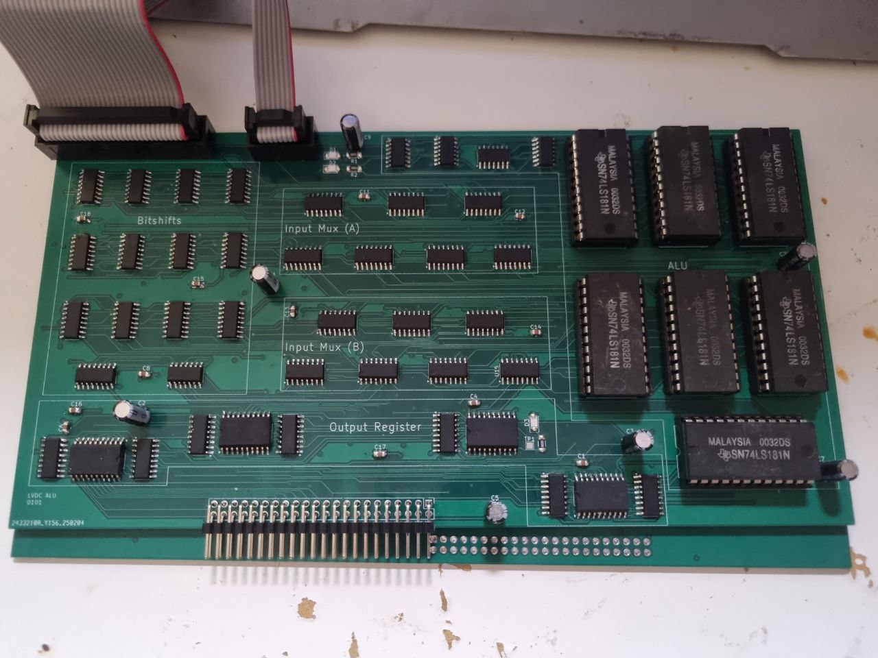
This was the first PCB I designed for the project. At its heart is a heap of 74LS181 ALUs, of which 7 are required to implement a full 26-bit ALU. All operations except for bitshifts are implemented through these. For shifts, a heap of 4-to-1 multiplexers select between the four possible shifts, which is a bit brute-force, but works. Conveniently, the multiplexers output a constant zero if their enable line is deasserted, providing the accumulator clear operation. Annoyingly, RSU exists, which is the same as SUB, but swaps the inputs around. The 74LS181s do not provide this, so the only way to implement this on this PCB so far is it to buffer both ALU inputs through 2-to-1 multiplexers to allow them to be conditionally swapped. That is 14 extra chips for all 26-bits, just for one instruction. Since one ALU input is the bus contents and the other is the accumulator, the result of the ALU computation needs to be latched and held until the ALU gets its turn to put this data onto the bus. A final set of multiplexers selects between 74LS181 and shifter outputs and this is then clocked into a set of D-Flip-Flops, which hold this data for just one clock cycle. But this is enough for the ALU output to be transfered over the bus.
Registers
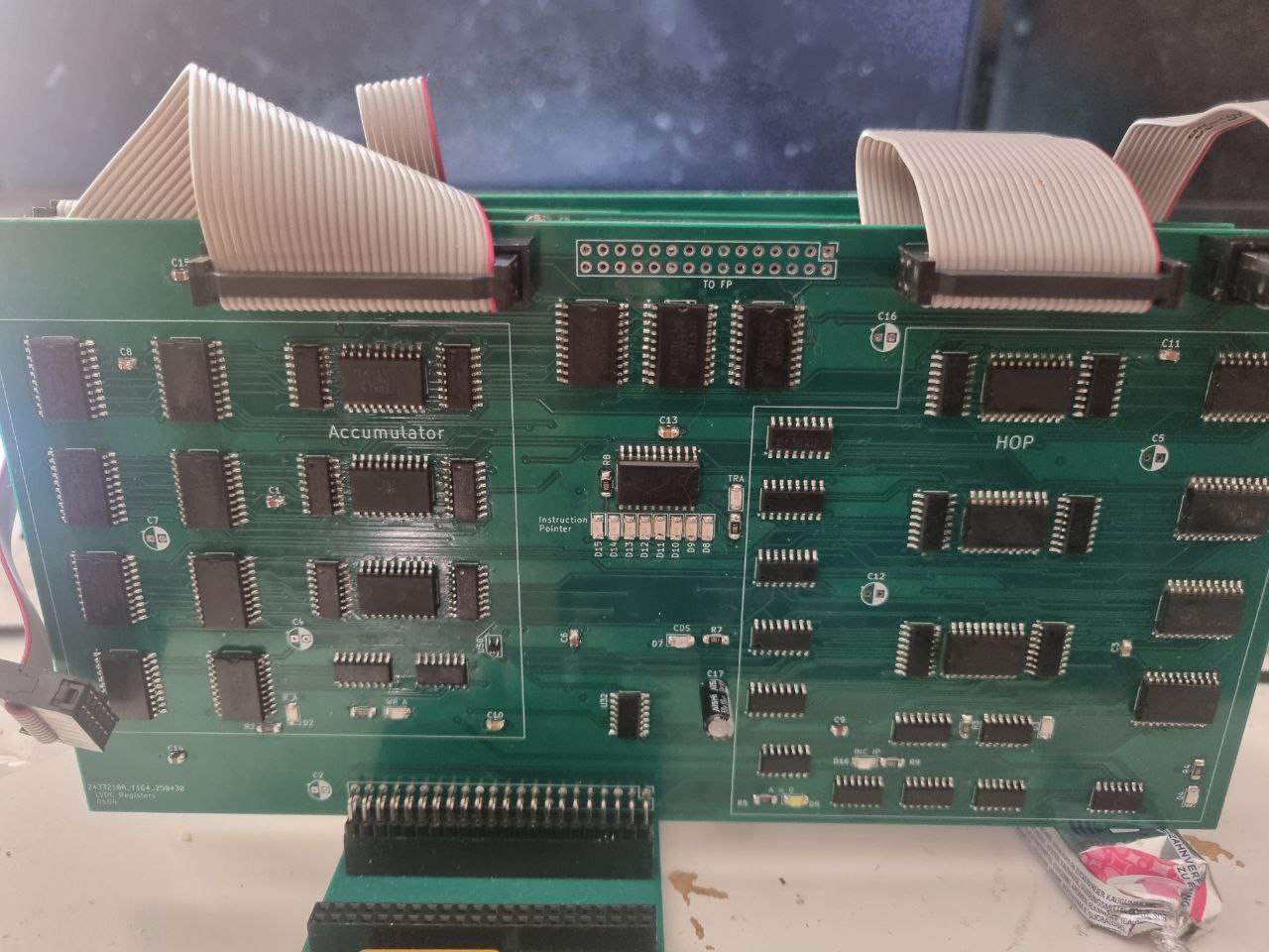
The register board holds the programmer visible registers, so the accumulator and HOP. One thing I tried to take with me from designing ICs was to avoid clock gating whereever possible and instead combine each D-Flip-Flop with a 2-to-1 multiplexer to select between new and old data, and this is the case here too. This leads to a very recognizable structure on all of these PCBs of 90° rotated, wide SO-20 packaged 74HCT574 D-Flip-Flops, flanked on the left and right by thin SO-16 packaged 74HCT157 multiplexers. As 26-bits does not divide by the 8-bits of the 74HCT574, the final two bits are often implemented through a 74HCT74 instead. The accumulator is also constantly checked against zero by 74HCT688s, for use by the TNZ instruction. TMI just checks the most-significant bit of the accumulator to determine signedness (the LVDC is a two’s complement machine, interestingly). HOP is a little more complicated as portions of it can be updated independently. For instance, the data selectors may be changed by CDS and the Instruction Counter by TRA. The whole thing may also be loaded from the bus, or may not change at all. Additionally, the Instruction Counter needs to be able to increment to step through instructions. So, a whole tree of multiplexers guide and arrange data into the HOP bits. To make matters more complicated, executing a STO instruction to one of two special memory locations actually stores HOP instead of the accumulator, to allow subroutine and interrupt linkages as described earlier. But this doesn’t store HOP as it is now, but as it would’ve been if no branch had taken place. So HOP is actually double-buffered, with a second set of D-Flip-Flops constantly being loaded from HOP as HOP updates, holding the previous value of HOP. This is what is then stored.
The accumulator value is actually exposed on a pin header labeled "TO FP" (to Front Panel) for display, but this later went unused. It is of note, though, that whenever things are exposed like this or wired to LEDs, it is always done through buffers. No LEDs or testpoints are wired directly to lines that also wire to logic inputs, to preserve signal transition times and noise margins.
Memory
-9f04aa43fb0bd048e5b87b20f8079000e9c04f431811e0d9a05779faf5a4c1c7.jpg)
This is actually the simplest PCB in the whole computer and the only two-layer PCB (every other module is a 4-layer board). On the original LVDC, core memory was used, which has the advantage of being random-access while also being non-volatile. In other words, the memory could be pre-loaded with software and the data would persist across power cycles while also being entirely read/write. Nowadays, this could’ve been accomplished using non-volatile memory technologies such as FRAM, but this would’ve been costly and required special logic for interfacing these chips to the system bus. Instead, I read that the LVDC did have memory sectors that were read-only. Writes to these sectors would simply be blocked, even though the memory itself supported writes. So if the LVDC can have ROM, so can I. 2048 addresses of EEPROM mapped into the first 4 sectors of module 0, with the entire remaining address space being SRAM.
Four 8-bit wide memory chips of which the excess 6 bits are hard-wired to zero are used for the writeable memory. The ROM is actually only two 8-bit wide chips. ROM accesses only define the least significant 16 bits of the full 26-bit word, with the remainder being hardwired to zero. This is okay, though, as instructions are only 13-bits wide, so the computer can still be programmed like this as long as instructions are only ever fetched from the low Syllable of ROM. It does put a cap on constant data values in ROM, but that will be okay for implementing a simple bootloader.
Control
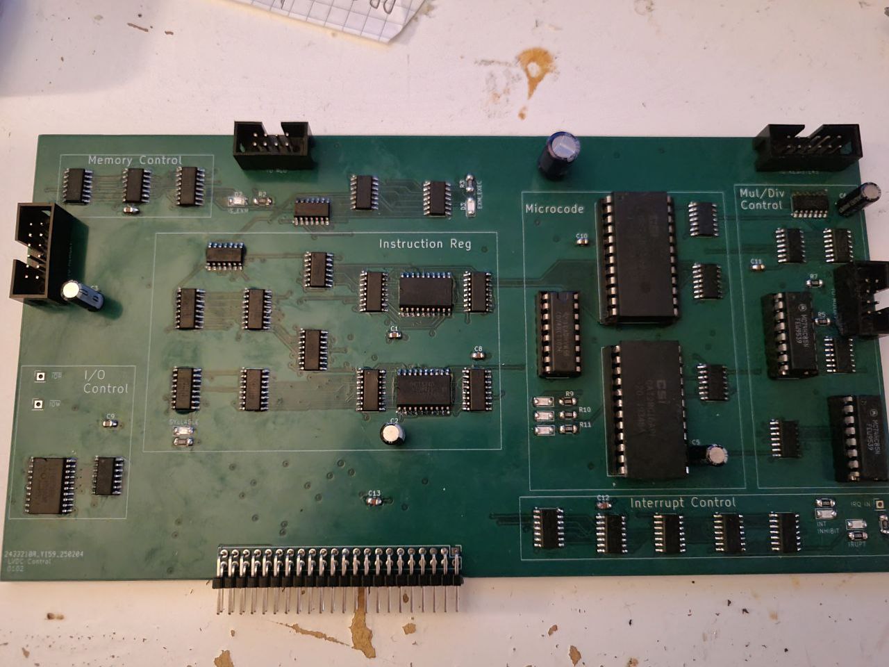
The control board ties everything together, containing the instruction decode unit generating all the control signals, as well as handling interrupts. The system is microcoded through two 2KiB EEPROMs which take in the instruction opcode from the Instruction Register (also on this board) as well as relevant instruction argument bits and the value of the 3-bit instruction cycle counter. Instructions can complete in varying amounts of time as there is a control signal to reset the cycle counter and fetch the next instruction. The shortest instructions complete in 3 clocks while the longest single instructions complete after 6 clock cycles, those being DIV and MPY. Most instructions complete after 4 clocks. Technically, MPH and EXM compete for longest instruction, but the former only as it halts the processor entirely until the multiplication is complete and the latter only because it triggers the out-of-order execution of another instruction. The maximum clock speed appears to be around 2.5MHz.
EXM became incredibly troublesome on this board. Not only because it causes the next instruction to be fetched out-of-order, but because the bits of this instruction are modified with ones from the EXM, which takes extra logic. But also, the incrementing of the Instruction Counter and the triggering of interrupt handling need to be inhibited the whole time. Normally, the control board checks for interrupts at the end of every instruction, but this of course shouldn’t happen in-between EXM and the instruction EXM is executing. Its a lot of logic for an instruction that still makes no sense to me. Seriously. I have yet to find a use for EXM in the code I’ve been writing for this machine. It is incredibly frustrating how much simpler the system design would be without EXM.
As for those interrupts, any request for one first triggers the setting of the Interrupt Pending latch to be handled at the end of the current instruction. When this latch is set, then the instruction fetch still goes ahead as usual, but a HOP referencing the interrupt vector address is forced into the Instruction Register and the Instruction Counter is not incremented. The interrupt is then marked as handled successfully, but no new interrupts are accepted until the Interrupt Pending latch is cleared by writing any value to a specific IO address. This is the only IO location that is decoded on a board other than the GPIO board and the only IO location also used for the same purpose on the original LVDC.
There is another problem, however, as backing up a return address in a subroutine involves storing HOP after a branch. Well, if an interrupt came in right between the instruction taking the branch and the instruction storing HOP, the computer would be in trouble as HOP would be corrupted once the interrupt returns and the HOP store tries to execute. I realized this a bit late, leading to the biggest bodge on any of the boards: inhibiting interrupts briefly after every taken branch. I actually have no idea if the original LVDC handled this problem in the same way, but I can’t really imagine a different way that they could’ve pulled off with the hardware at the time.
Bus Monitor
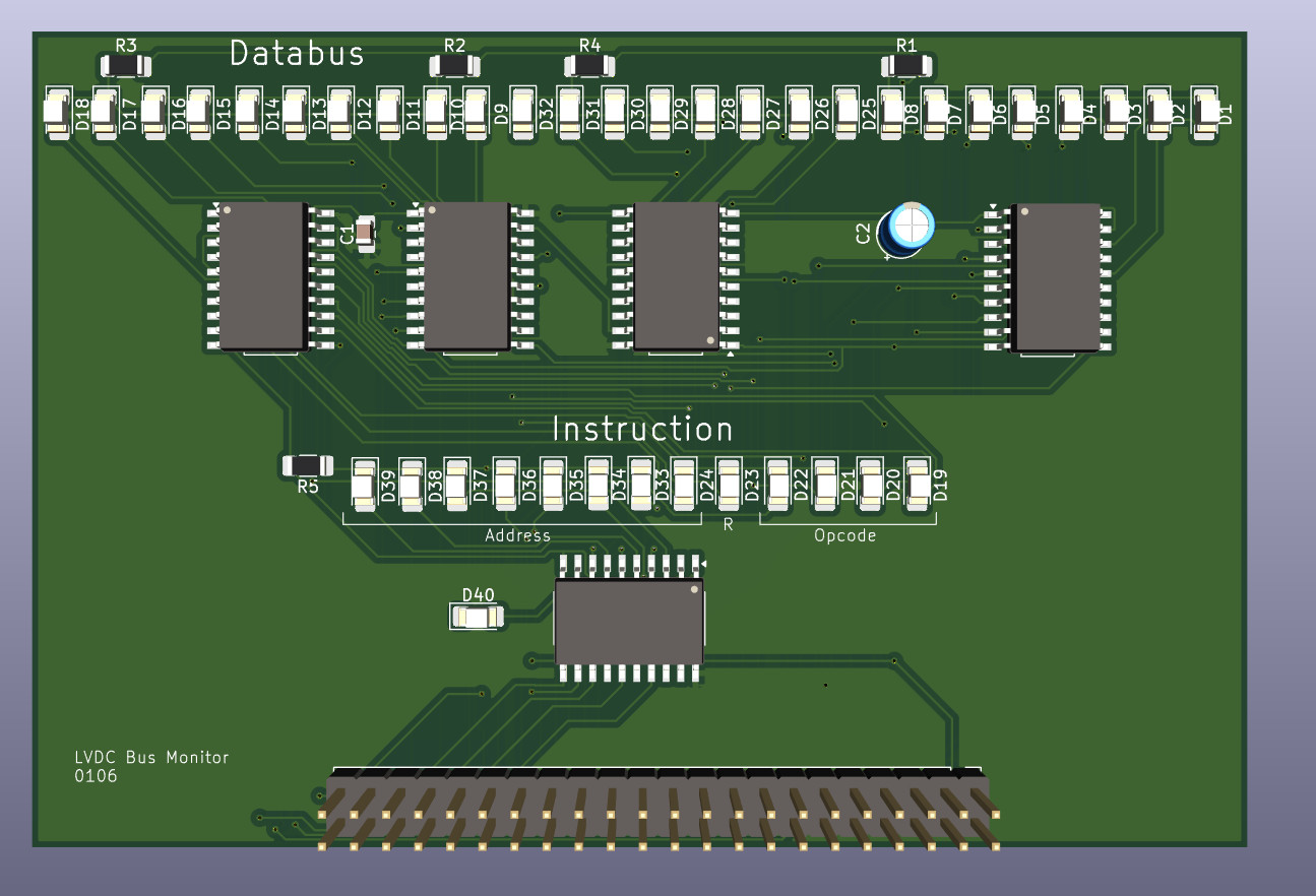
A simple bus monitor consisting of LEDs isolated by buffers to show the current bus value and instruction. As mentioned before, all LEDs must be buffered, so that is happening here too. The unlabeled LED shows the clock.
Backplane
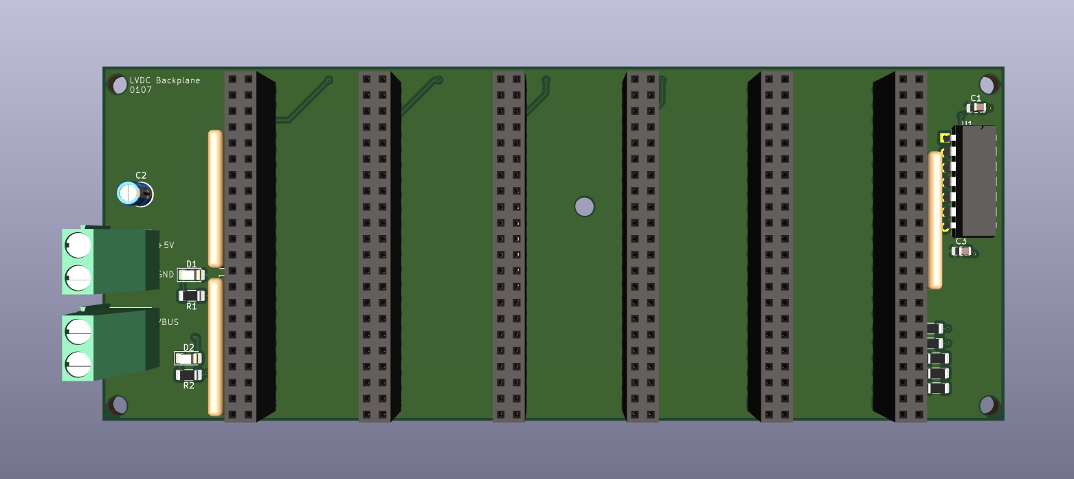
This is the PCB that every other module plugs into, mostly just featuring straight connections between the headers, technically allowing the modules to be plugged in in any order. The only constaint is that the backmost card must generate and output the system clock signal, rather than taking it as an input.
Only the most common signals are carried through the backplane. Signals that only need to travel between two specific modules are carried via ribbon cables between the modules involved. To improve bus speeds, any signals that travel through the backplane may be run at a higher voltage than the rest of the system, with buffers on each module boosting or lowering the voltage of these signals, thus the two screw terminals for power input. In my final system configuration, I ended up running both from the same +5V supply, though.
The slight bit of circuitry at the far end of the PCB is the clock buffer, another thing I translated from IC layout. Instead of every single Flip-Flop and counter in the whole system sharing one single clock line, a 74HCT04 containing 6 inverters generates 5 individual clock signals from the source clock. As all inverters are on the same IC, they should be evenly matched in delay, reducing clock skew. By giving each module its own clock source, the integrity of the clock signal is improved. The rising and falling edges are both steeper as there is less capacitance per clock line.
GPIO
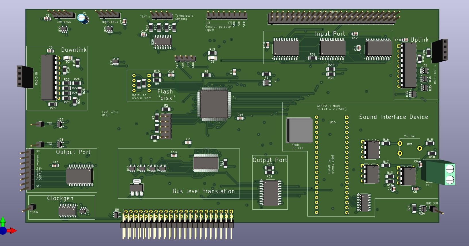
This board is where things go off the rails as its where I could put all of my custom peripheral choices without being restrained to historical accuracy. To drive this point home, the center of this board is a modern-ish CPLD, which mostly just generates control signals to the other peripherals, but itself contains an SPI port, system timer and front panel driver. The actual peripherals are pretty diverse, starting with simple digital input and output ports, followed by a radio transciever based on the HT12E/HT12D chips, a header to connect addressable LED strips to and a whole Commodore 64 SID chip in the form of my GFMPW-1 custom silicon.
The HT12E/HT12D combo allows 4 digital signals to be automatically transmitted and received over radio. The CPLD implements a serial protocol over these where 2 of the lines are data bits and one line is a clock bit, like SPI but two-bit, with the remaining bit containing a checksum that is simply the XOR of the two data bits. Any combination of bits with an invalid checksum acts as a transmission reset. A complete transmission of 16-bits being received can then trigger a CPU interrupt. I was supposed to build a corresponding transceiver to plug into my laptop, but ran out of time, so this feature is actually untested currently.
There is also a header on this board to connect temperature sensor modules to, to sense if the temperature inside the computer gets too high. If any one trips, this condition is communicated to the CPU through a status register. This register is regularly checked whenever the system timer triggers a regular interrupt about 7.6 times per second.
To provide persistent storage, a "disk" is also present on this board in the form of a 4MiB spiflash IC. Inconveniently, this memory uses 8-bit bytes as the base unit, not 26-bit words. So, again, every four bytes provide one 26-bit data word with 6 bits unused. But to make things faster, the SPI port in the CPLD implements a 16-bit wide receive data buffer, allowing faster data transfers out of the flash, the CPU only having to assemble two 16-bit words rather than four bytes. This is the limit, however, as, just like the ROM, the GPIO board only uses 16 bits of the databus, hardwiring the most-significant 10 to zero.
The clock is also generated here by dividing an input clock signal by 4. The GPIO board itself runs from the source clock, but the LVDC CPU runs from the divided clock.
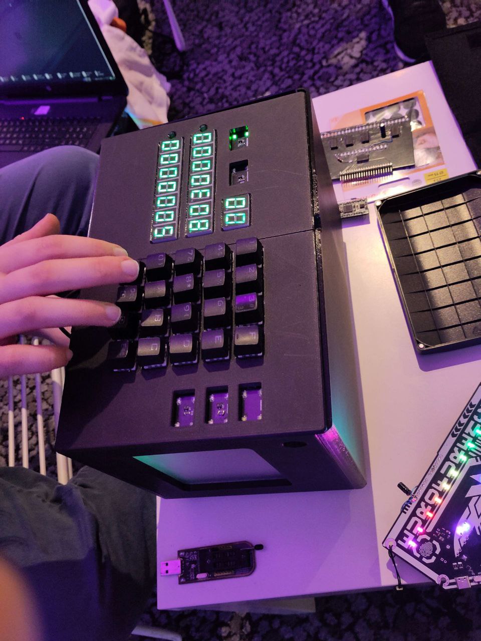
Front Panel
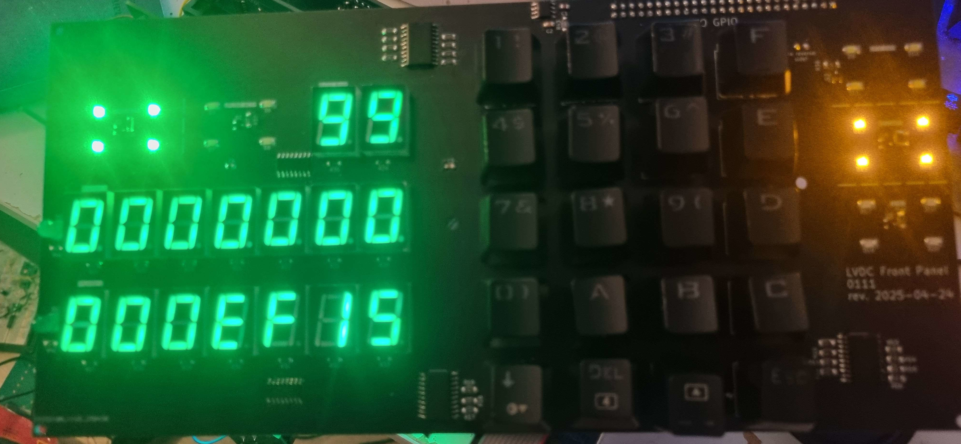
The front panel is intended to be reminiscent of the AGC’s DSKY, but with a hexadecimal-capable keypad. The keys are Cherry MX Blue switches salvaged from a mechnical keyboard and the displays are simple LED 7-segment displays. The LEDs to the left of the displays indicate if a number is negative or blink if input is required. The indicator lights are intended to have pieces of transparent foil with a label printed on them fitted to cutouts in the case above. Various buffers allow all lights to be multiplexed and driven by the 3.3V CPLD while boosting the voltage to the lights to 5V. All keys are directly readable by the CPU through one of the input ports, but the "Clear" key is special as it triggers an interrupt when pressed. It is a very high priority input as it indicates the operator wishes to input a command into the system, while the remaining keys are only read on-demand by the CPU.
Temperature Sensor
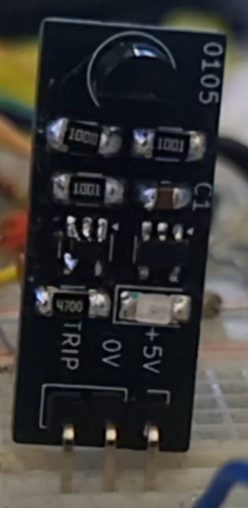
Five of these temperature sensors are distributed throughout the case and each is a relatively dumb device with a binary output. A temperature sensor, analog comparator and schmitt-trigger inverter cause a logic one to be emitted on the "TRIP" output if the temperature exceeds ~54°C and stays like this until the temperature has fallen again by several degrees. The module must actively pull the "TRIP" line low to stop the CPLD on the GPIO board from communicating a overtemperature condition to the CPU. If the line floats, such as if a component fails or the physical connections to the sensor sever, it immediately trips the overtemperature detection. There is a "TEMP" light illuminated by red LEDs on the front panel that is intended to turn on upon such a condition.
Case
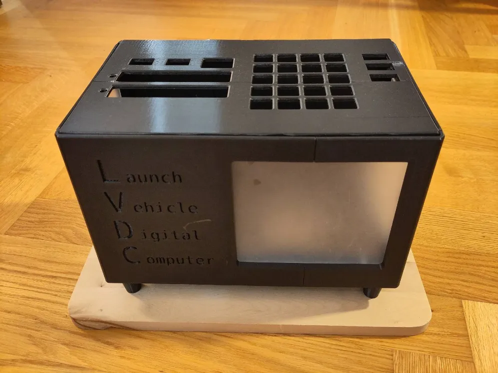
The case for the computer is 3D printed, but unfortunately each of the longer panels consists of two pieces as the whole thing ended up too wide, so it likes to fall appart. Not seen here is the fan mounted at the bottom of the case. To make matters worse, I do not own a 3D printer of my own and so instead I organized the printing be done by someone else, with us meeting at a convention and assembling everything in a comfy corner somewhere, hoping it all fits first-try. Luckily, it did, but I barely made it home with the case still in one piece. Not seen here is a later addition of an addressable LED strip controlled by the CPU which wrapps its way around both the inside and the outside of the case.
Multiply/Divide
I did not have the time or money to fully design and assemble the hardware multiply/divide board. Luckily, I designed the computer from the start to allow this board to be optional and I do have a proof-of-concept built up in Logisim Evolution using 74LS181 ALUs, some shift registers and minimal control logic to implement a multiply/divide circuit of a similar style to the CDP1855. It is important that 74LS181s are used here instead of simple adders, as one of their operations allow for one of their A inputs to be left-shifted one position, simplifying the circuit greatly.
Interestingly, this circuit is better then that of the original LVDC, which prioritized speed over precision and speed up the multiply/divide operations by approximating, leading to error in the least-significant two bits of the result. The circuit I designed, however, produces perfect results. Maybe one day, I will finish designing the schematic and PCB in KiCad, but things keep coming up...
Software
I had to speedrun the software a bit, but I still think I came up with a decent simple general-purpose operating system. The first step after power-up is bootloading from the spiflash, initializing all of SRAM starting at module 2. However, this requires indirect addressing, reading and assembling words from the flash and storing them at the address pointed to be an incrementing pointer. This is when the greatest trick I came up with for this computer comes in: self-modifying code. As the ROM is read-only, bytecode for a short subroutine is procedurally generated into the residual sector, consisting of a CDS to set the data module and sector from the most-significant bits of the pointer and a STO referencing the least-significant bits of the pointer. This takes a lot longer to fully execute on all targetted SRAM locations than it should, but still only takes a fraction of a second to complete. I’m not even sure if any of this was intended by the LVDC’s designers. One of the LVDC’s predecessors, the OBC, didn’t even have the ability to dynamically call subroutines (HOP cannot be stored on these machines). These were features that were simply not required for completing fixed mathematical computations and integrations. I only need them because I am doing something other than solving math problems with my computer!
After bootloading, things get easier, though, as all memory is now writeable. The last thing the bootloader does is write a interrupt vector to the same interrupt handler into every module, fully putting the system into a ready-to-go state, and branching to a location in SRAM. From here on, indirect addressing becomes possible by modifying upcoming instructions rather than writing out a whole subroutine. The system is now running what I just call the "LVDC Interactive System Software". It uses the regular system timer interrupt to update the displays and check the GPIO status register and contains a handler for common commands. If the operator wishes to launch a piece of custom software, a "Major Mode" program, it is loaded on-demand into a specific memory module, initialized and its loop function regularly executed. Only one of these may be active at a time.
The memory layout of the System Software is segmented by module. Module 0 is unused except for its residual sector, which holds system global variables ("globals"). Module 1 holds the bytecode of the current Major Mode (if any), Module 2 holds the interrupt handler bytecode, Module 3 holds the bytecode for the main program loop which ties everything together, Modules 4 and 5 hold the bytecodes for the various commands that may be issued by the operator, Module 6 holds common general-purpose subroutines and Module 7 is unused and may be used arbitrarily by Major Mode programs.
Interacting with the system software after successful final assembly.
If the "CLEAR" key is pressed, the System Software enters command entry mode, where it asks the user to first enter a 8-bit command code and hit "ENTER", optionally followed by a 26-bit command argument (if required). Commands may execute a single task immediately and then quit (i.e. "1C - Reset Alarms") or launch a continuous process (i.e. "26 - Monitor Memory Location") which can then be terminated by entering any other command ("01 - NOP" exists to just terminate the current command without doing anything else). Each command goes through three phases: "initial" on first run, followed optionally by "loop", called regularly, and ending on "final" when the command is being terminated. Commands may set themselves to be inactive to terminate themselves at any time.
The main program loop cycles between calling the command entry handler (if active), current command code (if active) and Major Mode code (if active). Since any one of these might want to set the contents of the displays, they don’t interact with this hardware directly and instead set global variables with the data they wish to display. The regular system timer interrupt then pushes these to the real displays based on a priority system. The command entry handler has the highest priority. Its user interface must always display if active. Then follows the current running command, as these may display information that the operator has explicitely asked for in this moment and last is the Major Mode display.
Major Modes are loaded from flash as needed and follow a similar pattern to commands on how they are executed in phases. They interact with the rest of the system by manipulating global variables in the module 0 residual sector, or by calling system functions. As the HOP instruction can load HOP from words stored in memory, a LUT of HOP values for all public subroutines allows for this.
This completes pretty much the simplest operating system I could think of and implement. It works well enough for me to run some demonstrations at least and create Major Mode programs to have fun with some of the peripherals (mostly the addressable LED strip).
Fun Issues
A whole circuit got added on to make the CPU inhibit interrupts briefly after taking a branch.
Of course, no project is without its problems. I actually tried to preempt this by simulating the whole thing beforehand. I found a KiCad plugin that can export your schematics as Verilog modules. It needed some updating, but I was able to use this to testbench the whole machine after writing some modules simulating all the 74-series and other chips I used. I ended up with a mostly bug-free design, but of course, even if the testbench says everything is up to spec, that doesn’t help if the spec is wrong, something I learn over and over again these days.
I already described how I needed to add bodges to inhibit interrupts on branches, but there is one bigger failing that can’t be fixed through bodges, and it involves HOP. As described earlier, storing HOP is supposed to store the value it would’ve taken on if the Instruction Counter incremented normally and none of the memory settings changed. However, my implementation simply stores the previous instruction’s version of HOP. The difference between those two is the Instruction Counter. The way I’m doing it, the Instruction Counter in the stored HOP is that of the previous instruction, not the instruction linearly following the previous instruction. So, attempting to store HOP after a branch and then loading HOP from the stored value just leads back to the branch instruction, creating an infinite loop. Ouch!
This requires a software workaround, since simply loading the stored HOP value and adding one to the Instruction Counter before loading it back into HOP fixes the problem, but, sadly, breaks compatibility with the original LVDC. One day, I will get a fixed PCB to amend this, but for now, I just have to use the software workaround.
My usage of 28C16 EEPROMs for the program ROM and the CPU microcode was definitely a mistake. They may be small and have the right capacity for the job, but also have a propagation delay time of 150ns. Not ideal. I believe this computer can go way above 2.5MHz if this bottleneck could be eliminated.
Project files and references
This project has its own repo here. Note that all PCB layouts and schematics contain my bug fixes except the HOP store issue, for which I have yet to come up with a fix.
I’d definitely like to thank the maintainers of The Virtual AGC Project. Their page on the LVDC contains pretty much all known information about the LVDC, or further references to such information. It was my primary source during this project.